A kind of annealing method of iii-v group semiconductor wafer

A III-V, semiconductor technology, used in semiconductor/solid-state device manufacturing, electrical components, circuits, etc., can solve the problems of difficult to eliminate the risk of debris, increased damage rate, proportionally increased debris risk, etc., to eliminate the risk of high temperature debris , the effect of reducing impact and reducing the risk of debris

Active Publication Date: 2021-07-27
苏州长瑞光电有限公司
View PDF6 Cites 0 Cited by
  • Summary
  • Abstract
  • Description
  • Claims
  • Application Information

AI Technical Summary

Problems solved by technology

The larger the wafer size during the process, the greater the longitudinal deformation caused by the same thermal stress (compared to the small-sized wafer), and the risk of fragmentation caused by the high-temperature annealing process increases proportionally. It is difficult to eliminate the risk of fragmentation in the existing annealing process, especially For the annealing process of 4-inch and above wafers, a damage rate of more than 10% will generally occur. As the wafer size increases, the damage rate will further increase

Method used


Image

  • A kind of annealing method of iii-v group semiconductor wafer
  • A kind of annealing method of iii-v group semiconductor wafer
  • A kind of annealing method of iii-v group semiconductor wafer

Examples


Embodiment 1

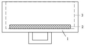
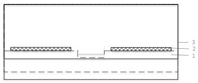
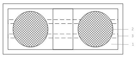
[0048] This embodiment adopts the most common annealing furnace, Figure 1 to Figure 3 shows how the wafer is loaded, such as Figure 1-Figure 3 As shown, the wafer 2 does not adopt the traditional way of placing the wafer boat in the vertical direction, but is placed horizontally on the loading table 1 made of quartz material. The table surface of the loading table 1 is treated as a smooth plane, which is consistent with The bottom surface of the wafer 1 is in full contact, and good heat conduction is realized between the wafer 2 and the loading stage 1. On the one hand, the force on the wafer 1 at high temperature is very balanced, and on the other hand, the temperature of the wafer 2 is adjusted with the load. The temperature of the wafer stage 1 changes synchronously. Since the thermal conductivity of the wafer stage is poor, its own temperature changes relatively slowly, so that the wafer 2 does not undergo a rapid temperature rise and fall. In the present embodiment, th...

Embodiment 2

[0051] The wafer loading method in this embodiment is the same as that in Embodiment 1, and will not be repeated here. The annealing temperature used in this embodiment is 420°C, Figure 5 The annealing process curve of this embodiment is shown. The first stage is a rapid heating stage, the wafer temperature rises from room temperature to 350 ° C, the heating rate is 33 ° C / min, and the heating time is about 10 min; In the initial stress release stage, the temperature is lowered to 300°C, and the cooling time is 1min; the third stage is the slow heating stage, the wafer temperature rises from 300°C to 420°C, the heating rate is 12°C / min, and the heating time is about 10min; the fourth The first stage is the constant temperature stage, the constant temperature is 420°C, and the constant temperature time is 15 minutes; the fifth stage is the slow cooling stage, the wafer temperature drops from 420°C to 300°C, the cooling rate is 12°C / min, and the cooling time is about 10 minut...


PUM


Abstract

The invention discloses an annealing method for III-V semiconductor wafers. In the heating stage of the annealing process, when the temperature rises to the first temperature in the temperature range of 300°C to 350°C, the temperature is increased by 30°C / min to 50°C. The cooling rate per minute should be lowered for no more than 1 minute, and then continue to heat up; in the cooling stage of the annealing process, when the temperature drops to the second temperature in the temperature range of 250 ° C ~ 300 ° C, the temperature should be 40 ° C / min ~ 50 ° C The heating rate is ℃ / min, and the heating time is not more than 1min, and then continue to cool down. Compared with the prior art, the invention can greatly reduce the damage rate in the wafer annealing process, thereby effectively improving the product yield.

Description

technical field [0001] The invention relates to the technical field of semiconductor manufacturing, in particular to an annealing method for III-V group semiconductor wafers. Background technique [0002] III-V group compound is a compound formed by B, Al, Ga, In of group III and N, P, As, Sb of group V in the periodic table of elements. The so-called group III-V semiconductor is composed of the above-mentioned group III The binary compound formed with group V elements has a chemical ratio of 1:1. III-V compound semiconductor materials have been widely used in optoelectronic devices, optoelectronic integration, ultra-high-speed microelectronic devices and ultra-high frequency microwave devices and circuits, and have broad prospects. The III-V semiconductors currently used in industry are mainly gallium arsenide (GaAs), indium phosphide (InP) and gallium nitride. [0003] III-V semiconductor wafers are currently mainly used in the fields of LED and LD. The process developme...

Claims


Application Information

Patent Timeline
Patent Type & Authority Patents(China)
IPC IPC(8): H01L21/324
CPCH01L21/324
Inventor 郭海侠薛金鹏周翔翔陈艳法
Owner 苏州长瑞光电有限公司
Why Eureka
Try Eureka