Microfluidic chip based on dielectrophoresis/electric infiltrate effect

A microfluidic chip and dielectrophoresis technology, applied in fluid controllers, laboratory containers, material analysis by electromagnetic means, etc. The effect of good scalability and low processing requirements

Active Publication Date: 2019-09-03
THE HONG KONG POLYTECHNIC UNIV SHENZHEN RES INST
View PDF12 Cites 1 Cited by
  • Summary
  • Abstract
  • Description
  • Claims
  • Application Information

AI Technical Summary

Problems solved by technology

[0010] In the prior art, the scheme disclosed in CN102430436 is to use the electrode arrays arranged in parallel horizontally and vertically to move a single droplet in the two-dimensional direction by applying an electric field, but the horizontal and vertical electrode arrays are on the same base ( That is, the lower base) is used to apply the driving voltage, and its upper base is a common ground without a pattern; because the common ground is used, it is only suitable for a single droplet (or multiple droplets that do not overlap horizontally and vertically) Otherwise, the manipulation of different droplets at similar positions will interfere with each other. For example, if two droplets with the same lateral position, if one wants to move up and the other wants to move down, it will be difficult to achieve

Method used


Image

  • Microfluidic chip based on dielectrophoresis/electric infiltrate effect
  • Microfluidic chip based on dielectrophoresis/electric infiltrate effect
  • Microfluidic chip based on dielectrophoresis/electric infiltrate effect

Examples


Embodiment 1

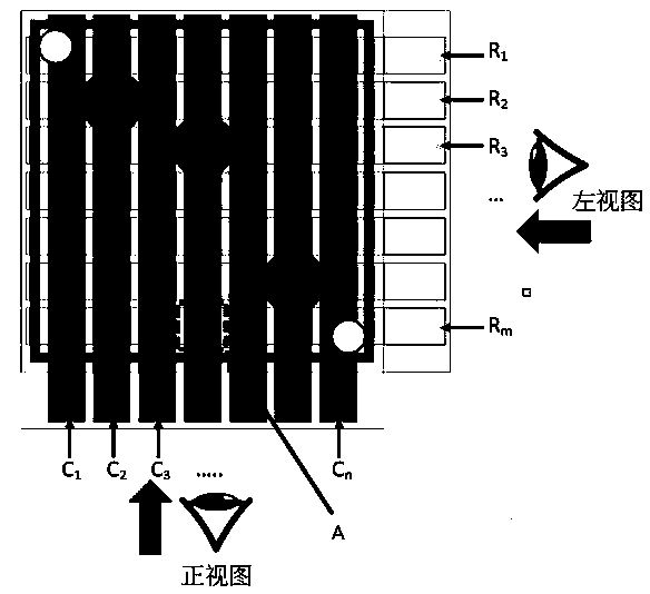
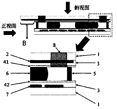
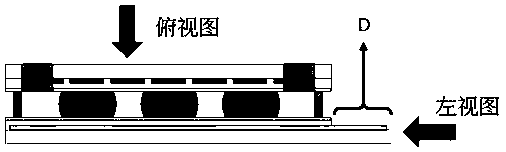
[0030] like Figure 1-3 As shown, a microfluidic chip based on the dielectrophoresis / electrowetting effect provided by the embodiment of the present invention, which is controlled by M + N microelectrodes to form an M×N microelectrode array, is characterized in that it includes a top-to-bottom Substrate layer 1, longitudinal electrode layer 2, dielectric layer 3, first hydrophobic coating layer 41, droplet layer 6, support layer 5, second hydrophobic coating layer 42, dielectric layer 3, and lateral electrode layer 7 stacked in sequence 1. Basal layer 1.

[0031] The vertical electrode layer 2 has a plurality of vertical metal lines, and each metal line is called a vertical driving electrode strip C1 , C 2 , C 3 … C n , referred to as the vertical strip; the horizontal electrode layer 7 has multiple horizontal metal lines, and each metal line is called a horizontal driving electrode strip R 1 , R 2 , R 3 … R n , referred to as horizontal bars. The electrodes in...


PUM

PropertyMeasurementUnit
thicknessaaaaaaaaaa

Abstract

The invention discloses a microfluidic chip based on dielectrophoresis / electric infiltrate effect. The microfluidic chip based on dielectrophoresis / electric infiltrate effect comprises a substrate layer, a longitudinal driving electrode layer, a dielectric layer, a hydrophobic coating layer, liquid drop layer, a hydrophobic coating layer, a dielectric layer, a transverse driving electrode layer, and a substrate layer which are laminated successively from top to bottom; the two hydrophobic coating layers are separated by a supporting layer; the longitudinal driving electrode layer comprise M longitudinal driving electrode strips; the transverse driving electrode layer comprises N transverse driving electrode strips; the transverse driving electrode strips and the longitudinal driving electrode strips are arranged in a vertically and horizontally staggered manner, and each staggered point is designed to be a control unit; the microfluidic chip is controlled by M*N driving electrode arrays. According to the microfluidic chip, using of external connection wires can be reduced greatly, so that independent control of electrodes in electrode array center part can be realized; and design and manufacturing are convenient.

Description

technical field [0001] The invention relates to a microfluidic chip, in particular to a microfluidic chip controlled by forming an M×N microelectrode array with M+N microelectrodes based on the dielectrophoresis / electrowetting effect. Background technique [0002] Microfluidic chips were first proposed by Manz and Widmer in Switzerland in the 1990s. It has many advantages such as low reagent consumption, small sample volume, fast analysis response, low energy consumption, easy integration and high-throughput analysis. Therefore, in the next 20 years, the scientific research community has invested a lot of energy in microfluidic At the same time, the industry is also further improving and producing microfluidic chips. At the same time, various microfluidic chip designs have been applied for patents one after another. [0003] Digital microfluidics is a new technology derived from microfluidics. In microfluidic technology, only one dimension of the fluid is required to reac...

Claims


Application Information

Patent Timeline
Patent Type & Authority Applications(China)
IPC IPC(8): B01L3/00G01N27/447
CPCB01L3/5027B01L3/50273B01L2300/0645B01L2300/0861B01L2300/0887B01L2300/165B01L2400/0424B01L2400/0427G01N27/4473G01N27/44752G01N27/44791
Inventor 张需明蔡智聪
Owner THE HONG KONG POLYTECHNIC UNIV SHENZHEN RES INST
Why Eureka
Try Eureka