A method for flip-chip bonding of ultra-thin wafer substrate chips with gold balls

A flip-chip welding and wafer technology, applied in the manufacturing of semiconductor devices, electric solid-state devices, semiconductor/solid-state devices, etc., can solve the problem that the packaging technology cannot meet the requirements of high density, and achieve simple design, high efficiency, and scope of application wide effect

Active Publication Date: 2021-03-23
NO 55 INST CHINA ELECTRONIC SCI & TECHNOLOGYGROUP CO LTD
View PDF7 Cites 0 Cited by
  • Summary
  • Abstract
  • Description
  • Claims
  • Application Information

AI Technical Summary

Problems solved by technology

[0002] With the miniaturization, light weight, thinning, high performance, increase in the number of I / O ports and the development of functional diversification of electronic products, traditional packaging technology can no longer meet the requirements of high density.

Method used


Image

  • A method for flip-chip bonding of ultra-thin wafer substrate chips with gold balls
  • A method for flip-chip bonding of ultra-thin wafer substrate chips with gold balls
  • A method for flip-chip bonding of ultra-thin wafer substrate chips with gold balls

Examples


Embodiment

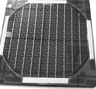
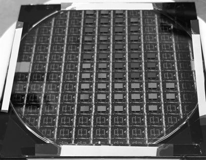
[0037] Chip gold ball flip-chip bonding test on a 4-inch GaAs wafer substrate with a thickness of 60 μm:

[0038] (1) Clean the 4-inch GaAs wafer substrate with a thickness of 60 μm with absolute ethanol, dry it in a 55°C oven for 10 minutes, and use hydrogen-argon plasma bombardment and inspection; clean the tooling carrier with absolute ethanol, and dry it in a 55°C oven 10min drying treatment;

[0039] (2) Place the 4-inch GaAs wafer substrate in (1) on the tooling carrier;

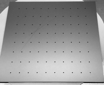
[0040] (3) Use high-temperature tape to paste along the four sides parallel to the tooling carrier, fasten the wafer substrate on the tooling carrier with high-temperature tape, and paste all the through holes in the tooling carrier with high-temperature tape;

[0041] (4) Use an automatic flip-chip mounter to flip-chip-bond the chip with the gold ball on the ultra-thin wafer substrate;

[0042] (5) The ultra-thin wafer substrate in (4) is diced by an automatic dicing machine.

[0043] It can be see...


PUM

PropertyMeasurementUnit
sizeaaaaaaaaaa
thicknessaaaaaaaaaa

Abstract

The invention relates to a method for flip-chip bonding of ultra-thin wafer substrate chip gold balls, comprising the following steps: (1) cleaning and inspection of the wafer substrate and cleaning of the tooling carrier; (2) placing the wafer substrate on the tooling carrier ; (3) Cut clean filter paper with the same width and size as the high temperature tape with a scalpel blade and other tools and paste the filter paper on the high temperature tape; (4) Paste the high temperature tape along the four sides parallel to the tooling carrier, and place the wafer The substrate is fastened on the tooling carrier with high-temperature tape, and all the through holes in the tooling carrier are pasted with high-temperature tape; (5) The chip with the gold ball is flip-chip welded on the ultra-thin wafer with an automatic flip-chip mounter (6) Scribing the ultra-thin wafer substrate by using an automatic dicing machine. Advantages: Effectively solve the problem of gold ball flip-chip welding of ultra-thin wafer substrate chips; simple design, strong operability, strong applicability, batch automatic production, and high efficiency.

Description

technical field [0001] The invention relates to an ultra-thin wafer substrate chip gold ball flip-chip welding method, which belongs to the technical field of micro-interconnection solder joint structure preparation, new material technology and semiconductor device manufacturing technology, and is for chips on ultra-thin wafer substrates. Gold ball flip-chip bonding offers a practical approach. Background technique [0002] With the miniaturization, light weight, thinning, high performance, increase in the number of I / O ports and the development of functional diversification of electronic products, traditional packaging technology can no longer meet the requirements of high density. The development of two-dimensional and three-dimensional stacking technology has brought hope for high-density packaging. High-density two-dimensional and three-dimensional stacking technologies often use gold balls (also known as gold bumps) or tin-based and indium-based solder balls to achieve...

Claims


Application Information

Patent Timeline
Patent Type & Authority Patents(China)
IPC IPC(8): H01L21/60H01L21/67
CPCH01L21/67132H01L24/81H01L24/94H01L2224/812
Inventor 田飞飞张君直周明
Owner NO 55 INST CHINA ELECTRONIC SCI & TECHNOLOGYGROUP CO LTD
Why Eureka
Try Eureka