Patterned electrochromic device, electrochromic glass and application
A technology of electrochromic devices and electrochromic glass, which is applied in the direction of instruments, nonlinear optics, optics, etc., can solve the problems of reduced response time of electrochromic glass, inability to present a sense of layering or gradient, and single display effect, etc. Achieve excellent electrochromic performance, easy processing technology, and broad application prospects
- Summary
- Abstract
- Description
- Claims
- Application Information
AI Technical Summary
Problems solved by technology
Method used
Image
Examples
Embodiment 1
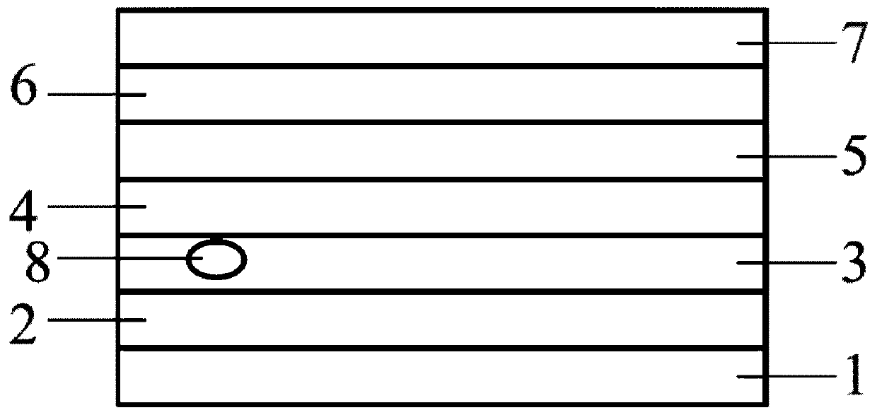
[0069] This embodiment provides a patterned electrochromic device, such as figure 1 As shown, the patterned electrochromic device includes a protective layer 1, a first conductive layer 2, an electrochromic layer 3, an electrolyte layer 4, an ion storage layer 5, and a second conductive layer from bottom to top. 6 and a reflective layer 7, wherein the electrochromic layer 3 is provided with a prefabricated pattern 8; the thickness of the protective layer is 2mm; the light transmittance of the protective layer is 90%; the thickness of the reflective layer is 2mm; the reflectivity of the reflective layer is 85% %; the thickness of the first conductive layer and the second conductive layer is 100 μm; the conductive material of the first conductive layer and the second conductive layer is ITO; the thickness of the electrochromic layer is 50 μm; the material of the electrochromic layer is polyaniline The electrochromic material; the thickness of the ion storage layer is 50 μm; the ...
Embodiment 2
[0075]This embodiment provides a patterned electrochromic device, the patterned electrochromic device sequentially includes a protective layer, a first conductive layer, an electrochromic layer, an electrolyte layer, and an ion storage layer combined together from bottom to top , the second conductive layer and the reflective layer, wherein the electrochromic layer is provided with a prefabricated pattern; the thickness of the protective layer is 0.7mm; the light transmittance of the protective layer is 92%; the thickness of the reflective layer is 1.1mm; the reflection of the reflective layer The ratio is 80%; the thickness of the first conductive layer and the second conductive layer is 25 μm; the material of the first conductive layer and the second conductive layer is ITO; the thickness of the electrochromic layer is 0.1 μm; the material of the electrochromic layer is Polypyrrole-based electrochromic material; the thickness of the ion storage layer is 0.1 μm; the material o...
Embodiment 3
[0081] This embodiment provides a patterned electrochromic device, the patterned electrochromic device sequentially includes a protective layer, a first conductive layer, an electrochromic layer, an electrolyte layer, and an ion storage layer combined together from bottom to top , the second conductive layer and the reflective layer, wherein the electrochromic layer is provided with a prefabricated pattern; the thickness of the protective layer is 3mm; the light transmittance of the protective layer is 98%; the thickness of the reflective layer is 3mm; the reflectivity of the reflective layer is 98%; the thickness of the first conductive layer and the second conductive layer is 200 μm; the material of the first conductive layer and the second conductive layer is conductive graphite; the thickness of the electrochromic layer is 100 μm; the material of the electrochromic layer is polythiophene An electrochromic material; the thickness of the ion storage layer is 100 μm; the mater...
PUM
| Property | Measurement | Unit |
|---|---|---|
| thickness | aaaaa | aaaaa |
| thickness | aaaaa | aaaaa |
| thickness | aaaaa | aaaaa |
Abstract
Description
Claims
Application Information
 - Generate Ideas
- Intellectual Property
- Life Sciences
- Materials
- Tech Scout
- Unparalleled Data Quality
- Higher Quality Content
- 60% Fewer Hallucinations
Browse by: Latest US Patents, China's latest patents, Technical Efficacy Thesaurus, Application Domain, Technology Topic, Popular Technical Reports.
© 2025 PatSnap. All rights reserved.Legal|Privacy policy|Modern Slavery Act Transparency Statement|Sitemap|About US| Contact US: help@patsnap.com


