


Quick Research
Generate reliable direction feasibility study reports for your R&D in just a few steps.

Technical Q&A
Discover and master advanced knowledge NOW. Basics, ideas, possibilities, all at once.

Find Solutions
As an expert in R&D theories, this can generate solutions to your technical problems instantly.

Evaluate Feasibility
Analyze your overall solution with one click, know your potential R&D risks in advance.

Monitor Landscape
Get weekly tech updates, stay abreast of the latest tech innovations and key insights.
Secondary electron detector, charged particle optical imaging equipment and detection method
A technology of secondary electron and detection method, which is applied in the field of scanning electron microscopy, can solve problems such as image distortion, and achieve the effect of improving precision and clarity
- Summary
- Abstract
- Description
- Claims
- Application Information
AI Technical Summary
Problems solved by technology
Method used
Image

Examples
Embodiment 1
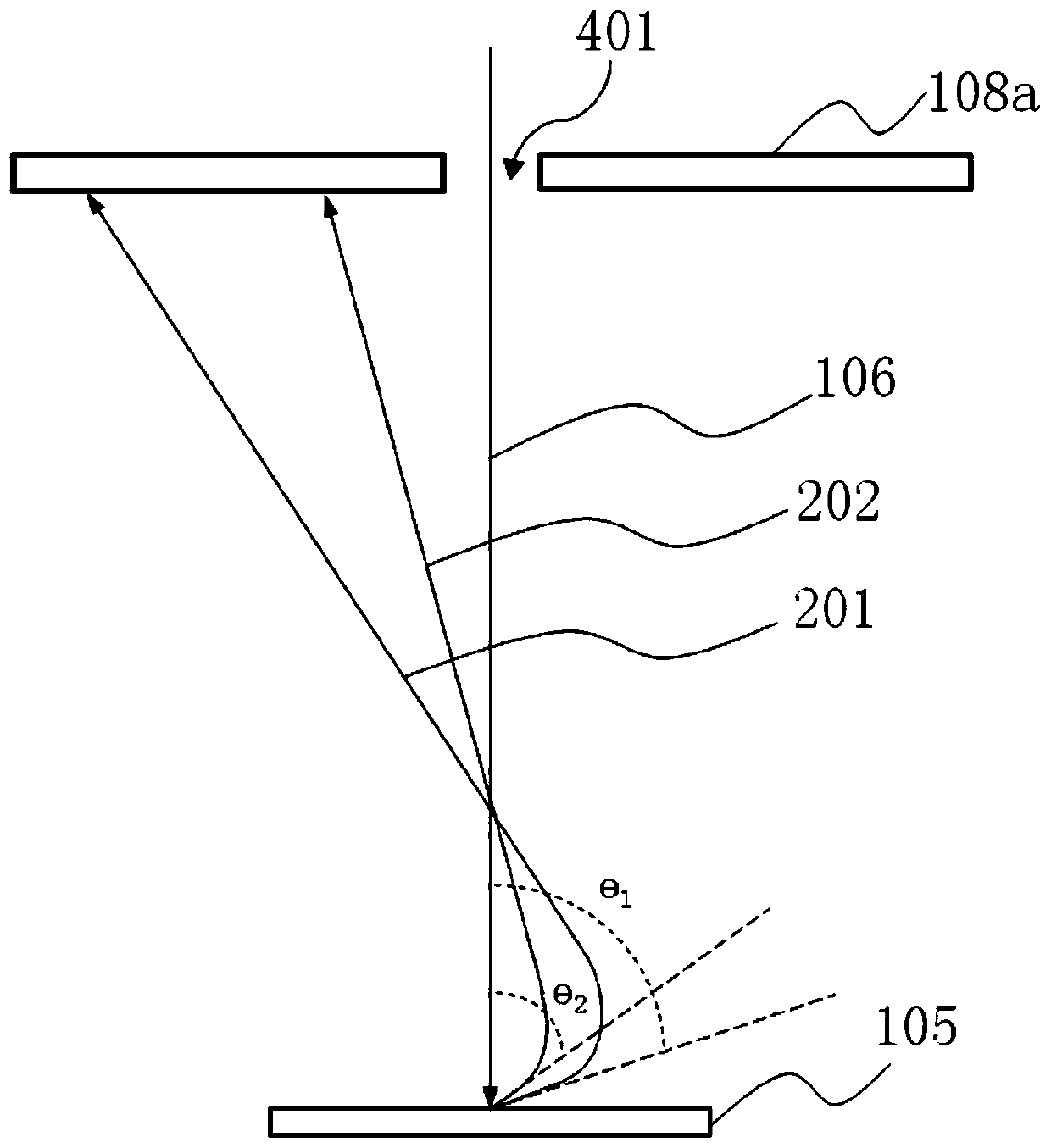
[0048] combine Figure 5 and refer to Figure 4 As shown, this embodiment discloses a secondary electron detector. The secondary electron detector is used to receive the secondary electrons (Secondary Electrons, SE) generated by the incident charged particle beam bombarding the surface of the sample 105, without receiving back scattered electrons (Back Scattered Electron, BSE), and through the two The signal amplification circuit and the analog-to-digital conversion circuit connected to the sub-electron detector present the microscopic topography of the surface of the sample 105 on the display device.
[0049] Based on the scanning electron microscope (SEM) assembled and formed by the secondary electron detector, the surface of the physical sample, microelectronic devices such as micron-scale and nano-scale semiconductor devices, optical integrated devices, microwave devices, quantum devices, or cell tissues are observed. The surface topography of the sample can be effective...
Embodiment 2
[0060] With reference Figure 6 Another modified embodiment of a secondary electron detector of the present invention is shown. The main difference between this embodiment and Embodiment 1 is that in the secondary electron detector disclosed in this embodiment, the circular detection area is radially divided into at least two isolated and fan-shaped first sub-detection areas according to the azimuth angle. , and further specifically, the circular detection area is divided into at least two annular first sub-detection areas that are equally divided and isolated.
[0061] The secondary electron detector is divided into several first sub-detection areas according to the azimuth separation, that is, the first sub-detection area 601 , the first sub-detection area 602 , the first sub-detection area 603 and the first sub-detection area 604 . Those skilled in the art can reasonably predict that the secondary electron detector can also be divided into two, three, five or more first su...
Embodiment 3
[0067] With reference Figure 7 Another modified embodiment of a secondary electron detector of the present invention is shown. The main difference between this embodiment and the secondary electron detector shown in Embodiment 1 and / or Embodiment 2 is that, in this embodiment, the central hole 401 is provided with a number of mutually isolated circular detection areas, and The radially outward portion of the ring detection area forms a second sub-detection area that is radially divided into at least two isolated fan-shaped sub-detection areas according to the azimuth angle. The circular detection area radially outward forms the second sub-detection area formed by radial division according to the azimuth angle, and the number may be two, three, five or any other number.
[0068] In particular, it should be noted that, Figure 7 It is only an exemplary solution of a secondary detector disclosed in this embodiment. As another reasonable modification, one or more annular detec...
PUM
 Abstract
Description
Claims
Application Information
 - R&D Engineer
- R&D Manager
- IP Professional
- Industry Leading Data Capabilities
- Powerful AI technology
- Patent DNA Extraction
Browse by: Latest US Patents, China's latest patents, Technical Efficacy Thesaurus, Application Domain, Technology Topic, Popular Technical Reports.
© 2024 PatSnap. All rights reserved.Legal|Privacy policy|Modern Slavery Act Transparency Statement|Sitemap|About US| Contact US: help@patsnap.com