Interference photoetching system, printing apparatus, and interference photoetching method
A technology of interference lithography and printing devices, which is applied in the field of interference lithography, can solve the problems of complex optical path construction, complex structure, and large structure, and achieve the effect of low production cost, simple structure, and variable-period interference lithography
- Summary
- Abstract
- Description
- Claims
- Application Information
AI Technical Summary
Problems solved by technology
Method used
Image

Examples
no. 1 example
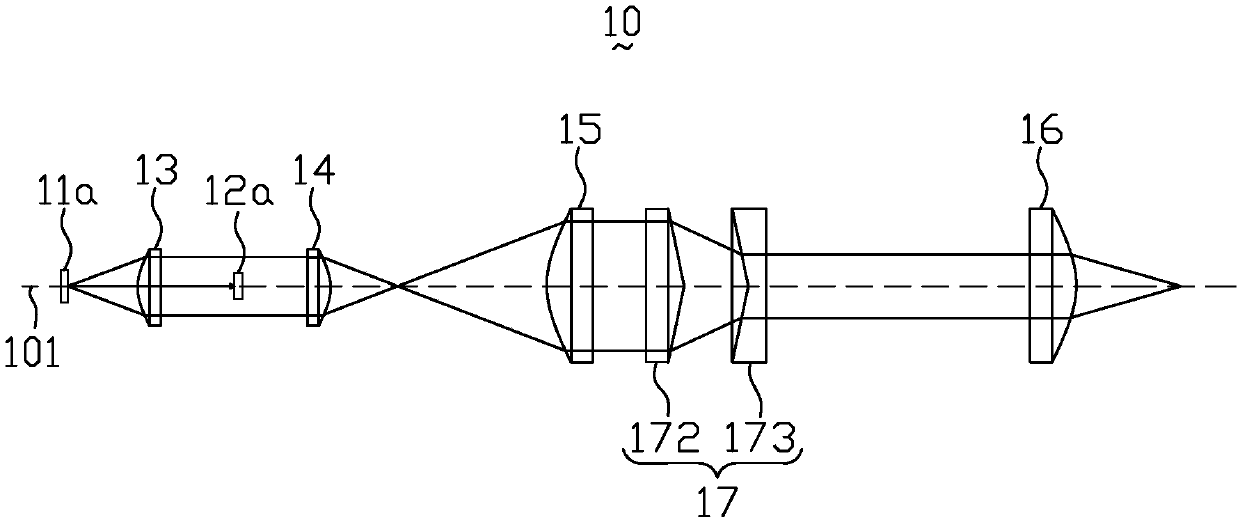
[0033] figure 1 is a structural schematic diagram of the interference lithography system of the present invention. Such as figure 1 As shown, the interference lithography system 10 includes a phase element 11 a, a light blocking diaphragm 12 a, a first lens 13 , a second lens 14 , a third lens 15 , a fourth lens 16 and an axicon lens group 17 .
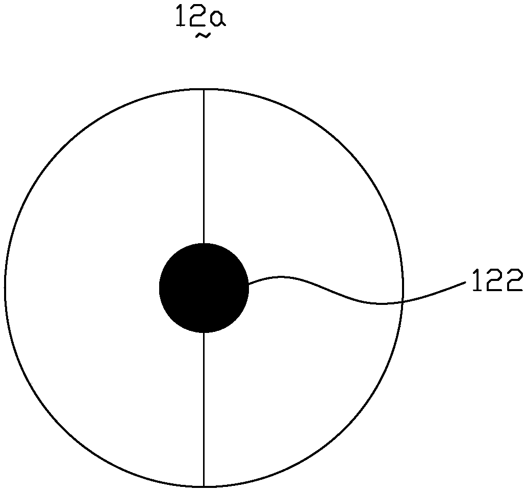
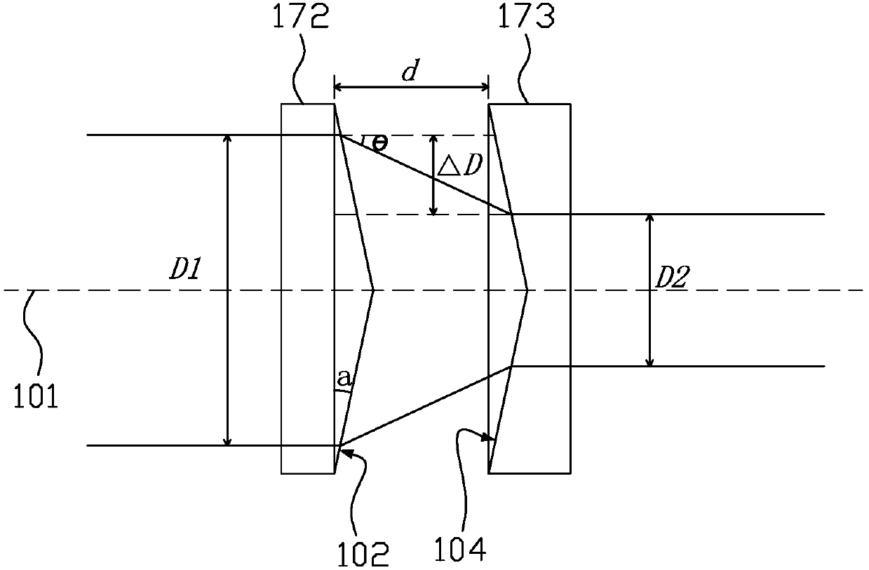
[0034] The phase element 11a, the first lens 13, the light-blocking diaphragm 12a, the second lens 14, the third lens 15, and the fourth lens 16 are arranged in sequence along the propagation direction of the optical axis 101, and the first lens 13 and the second lens 14 form a A group of 4F imaging systems, the third lens 15 and the fourth lens 16 form another group of 4F imaging systems, and the axicon lens group 17 is movably arranged between the third lens 15 and the fourth lens 16 along the propagation direction of the optical axis 101 . The phase element 11a is used to split the light beam, and the phase element 11a is a light...
no. 2 example
[0045] Figure 5 It is a schematic diagram of the partial structure of the phase element of the second embodiment of the present invention. Figure 6 It is a structural schematic diagram of the light-blocking diaphragm of the second embodiment of the present invention. Such as Figure 5 and Figure 6 As shown, the structure of the interference lithography system 10 of this embodiment is substantially the same as that of the interference lithography system 10 of the first embodiment, except that the interference lithography system 10 of this embodiment is used to realize multi-beam, multi-angle, variable Periodic interference lithography.
[0046] Such as Figure 5 and Figure 6 As shown, by changing the structural design of the phase element 11b and the light-blocking diaphragm 12b, multi-beam interference lithography can be realized. Specifically, the phase element 11b is provided with a plurality of hexagonal periodic structures 112 arranged in an array, and the light ...
no. 3 example
[0048] Figure 7 is a schematic structural diagram of a printing device according to a third embodiment of the present invention. Such as Figure 7 As shown, the printing device 100 includes the above-mentioned interference lithography system 10, a laser source 20, a beam shaper 30, a beam splitter 40a, a half mirror 40b, a detection optical path 50a, an autofocus optical path 50b, a miniature objective lens 60, and a translation stage 70, controller 80 and computer 90. In this embodiment, a beam shaper 30, a beam splitter 40a, a half mirror 40b, a miniature objective lens 60, and a translation stage 70 are sequentially arranged along the propagation direction of the laser light, wherein the detection optical path 50a is arranged on the transmitted light of the beam splitter 40a. On the way, the autofocus optical path 50b is set on the reflection optical path of the half mirror 40b.
[0049] The laser light emitted by the laser source 20 passes through the beam shaper 30 to...
PUM
 Abstract
Description
Claims
Application Information
 - Generate Ideas
- Intellectual Property
- Life Sciences
- Materials
- Tech Scout
- Unparalleled Data Quality
- Higher Quality Content
- 60% Fewer Hallucinations
Browse by: Latest US Patents, China's latest patents, Technical Efficacy Thesaurus, Application Domain, Technology Topic, Popular Technical Reports.
© 2025 PatSnap. All rights reserved.Legal|Privacy policy|Modern Slavery Act Transparency Statement|Sitemap|About US| Contact US: help@patsnap.com