Vibrating beam, manufacturing method of vibrating beam, and silicon micro gyroscope
A technology of vibrating beam and silicon wafer, which is applied in the direction of gyro effect for speed measurement, gyroscope/steering sensing equipment, measuring device, etc., which can solve the problem of difficult to guarantee machining accuracy, difficult process control, and flexibility of vibration beam spindle azimuth design. Low problems, to achieve the effect of high processing quality, improved mechanical sensitivity, and easy control
- Summary
- Abstract
- Description
- Claims
- Application Information
AI Technical Summary
Problems solved by technology
Method used
Image
Examples
Embodiment 1
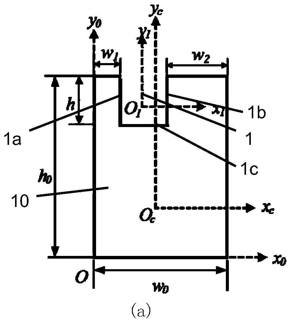
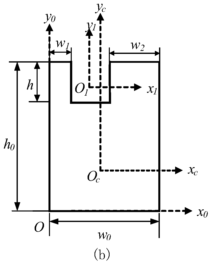
[0041] as attached Figure 2a , Figure 2b As shown, the embodiment of the present invention provides a vibrating beam, including a beam body 10, one side of the beam body is provided with a groove 1 along the depth direction, and the groove 1 has a first side 1a, a second side 1b and On the bottom surface 1c between the two sides, the groove 1 is arranged along the length direction of the beam body 10 .
[0042] Figure 2a , Figure 2b It is a schematic cross-sectional view of the vibrating beam. The groove 1 is formed by a downward depression on one side of the beam body 10. The groove 1 is opened along the length direction of the beam body 10. In an embodiment of the present invention, the groove 1 is formed along the beam body 10. The length direction of the upper side of the body 10 is set through, that is, the structure of any cross section of the beam body 10 is as follows: Figure 2a , Figure 2b As shown; in another embodiment of the present invention, the groove...
Embodiment 2
[0053] see Figure 5 In (a), a method for preparing a vibrating beam, the vibrating beam adopts the structure of the above-mentioned vibrating beam, and the method for preparing the vibrating beam includes:
[0054] Mask layers 101 are respectively generated on the upper and lower surfaces of the crystal-oriented silicon wafer 100; the profile of the crystal-oriented silicon wafer can be processed according to the cross-sectional shape and size of the vibrating beam, such as the formation of a single vibrating beam groove; A plurality of grooves are formed on the crystal-oriented silicon wafer at one time, and then a plurality of vibration beams are formed after cutting; the mask layer here is specifically a silicon dioxide film layer. In order to improve the surface quality, the upper and lower surfaces of the crystal-oriented silicon wafer 100 can be respectively polishing;
[0055] wherein a first photoresist layer 201 is coated on the upper mask layer 101; a first groove ...
Embodiment 3
[0076] see Image 6 , the embodiment of the present invention provides a silicon micro-gyroscope, including a silicon sensitive structure (see Image 6 a) and the silicon click structure used to drive the action of the silicon sensitive structure (cf. Image 6b), the silicon-sensitive structure includes a vibrating beam, a stress relief structure, and a mass connecting the vibrating beam and the stress releasing structure, and the vibrating beam is the vibrating beam of any of the above-mentioned embodiments.
[0077] The sensitive structure of the micromechanical gyroscope of the present invention is a flat capacitive type, and the working mode is electrostatic drive and capacitive detection. Two symmetrical large-area sensitive masses are designed, which have the advantages of high sensitivity and strong anti-interference ability. The stiffness of the vibrating beam determines the frequency of the driving mode, the detection mode and the motion characteristics of the vibra...
PUM
 Abstract
Description
Claims
Application Information
 - R&D Engineer
- R&D Manager
- IP Professional
- Industry Leading Data Capabilities
- Powerful AI technology
- Patent DNA Extraction
Browse by: Latest US Patents, China's latest patents, Technical Efficacy Thesaurus, Application Domain, Technology Topic, Popular Technical Reports.
© 2024 PatSnap. All rights reserved.Legal|Privacy policy|Modern Slavery Act Transparency Statement|Sitemap|About US| Contact US: help@patsnap.com


