Storage operation circuit module and processor
A computing circuit and computing unit technology, applied in the field of processors and storage computing circuit modules, can solve the problems of limited increase in processor data computing speed and layout restrictions, and achieve the effects of reducing power consumption, increasing computing speed, and reducing data transmission.
- Summary
- Abstract
- Description
- Claims
- Application Information
AI Technical Summary
Problems solved by technology
Method used
Image
Examples
no. 1 example
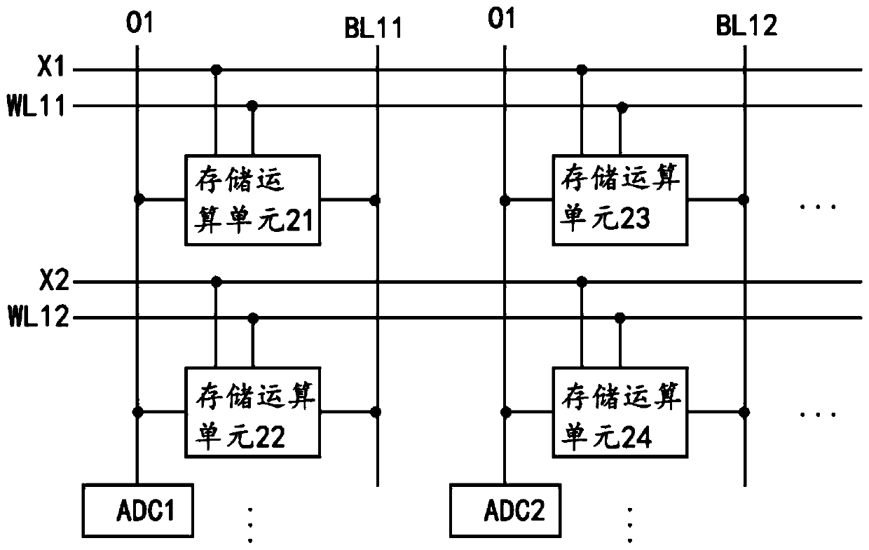
[0034] See image 3 The storage operation circuit module of this embodiment includes a plurality of storage operation units 21, 22, 23, 24, etc., the plurality of storage operation units are arranged in an array, and each storage operation unit is connected to the word line WL and the bit line BL , The word line WL is used to select a row of storage operation unit data for reading and writing, for example, the word line WL11 is used to select a row of multiple storage operation units where the storage operation units 21, 23, etc. are located, and the word line WL21 is used to select storage operation units 22, 24, etc. are located in a row with multiple storage operation units. The bit line BL1 is used to read and write the data of a certain column of storage operation units. For example, the bit line BL11 can select a column of storage operation units where the storage operation units 21, 22, etc. are located, and the bit line BL12 can select the storage operation unit 23. , 2...
no. 4 example
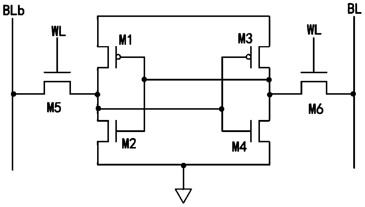
[0056] The storage operation circuit module of this embodiment includes a plurality of storage operation units. The difference from the first embodiment is that the structure of the operation storage unit of this embodiment is changed. See Figure 7 The arithmetic storage unit of this embodiment has a storage unit, a first switching device, a second switching device, a third switching device S4, and a capacitor C4 as a charge storage unit. The storage unit is the same as the storage unit of the first embodiment. It also includes multiple field effect tubes M41, M42, M43, M44, M45, and M46.
[0057] Different from the first embodiment, the first switching device M47 of this embodiment is an NMOS tube, that is, a high-level conductive switching device, and the second switching device M48 is a PMOS tube, that is, a low-level conductive switching device. . In addition, the first switching device M47 and the second switching device M48 both receive the operation data complementary si...
PUM
 Abstract
Description
Claims
Application Information
 - R&D
- Intellectual Property
- Life Sciences
- Materials
- Tech Scout
- Unparalleled Data Quality
- Higher Quality Content
- 60% Fewer Hallucinations
Browse by: Latest US Patents, China's latest patents, Technical Efficacy Thesaurus, Application Domain, Technology Topic, Popular Technical Reports.
© 2025 PatSnap. All rights reserved.Legal|Privacy policy|Modern Slavery Act Transparency Statement|Sitemap|About US| Contact US: help@patsnap.com


