
Image sensor, forming method thereof and camera module

An image sensor and device technology, which is applied in the direction of electric solid state devices, semiconductor devices, electrical components, etc., can solve the problem that the performance of image sensors needs to be improved.

Inactive Publication Date: 2019-07-30
ICLEAGUE TECH CO LTD
View PDF5 Cites 0 Cited by
  • Summary
  • Abstract
  • Description
  • Claims
  • Application Information

AI Technical Summary

Problems solved by technology

[0003] However, the performance of existing image sensors needs to be improved

Method used


Image

  • Image sensor, forming method thereof and camera module
  • Image sensor, forming method thereof and camera module
  • Image sensor, forming method thereof and camera module

Examples


Embodiment Construction

[0042] As mentioned in the background, the performance of existing image sensors needs to be improved.

[0043] A camera module usually consists of an image sensor chip and a lens. The optical path is defined as the distance traveled by light in a medium multiplied by the index of refraction. For an ideal lens, all light rays from the object point to the image point have exactly the same optical path. However, in actual situations, the lens is distorted and deviates from perfection. The distortion of the lens has a serious impact on imaging. For example, the imaging effect of the edge area of ​​​​the image sensor chip is worse than that of the center of the image sensor chip, including clarity and brightness. Wait. This difference in imaging effect is caused by the characteristics of the lens, and it is difficult to greatly improve the lens.

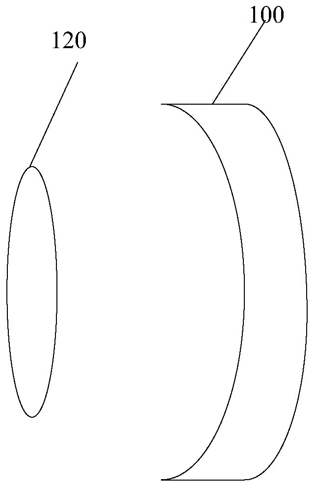
[0044] In order to improve the imaging effect of the edge region of the image sensor chip, an image sensor chip 100 in an arc shape ...


PUM


Abstract

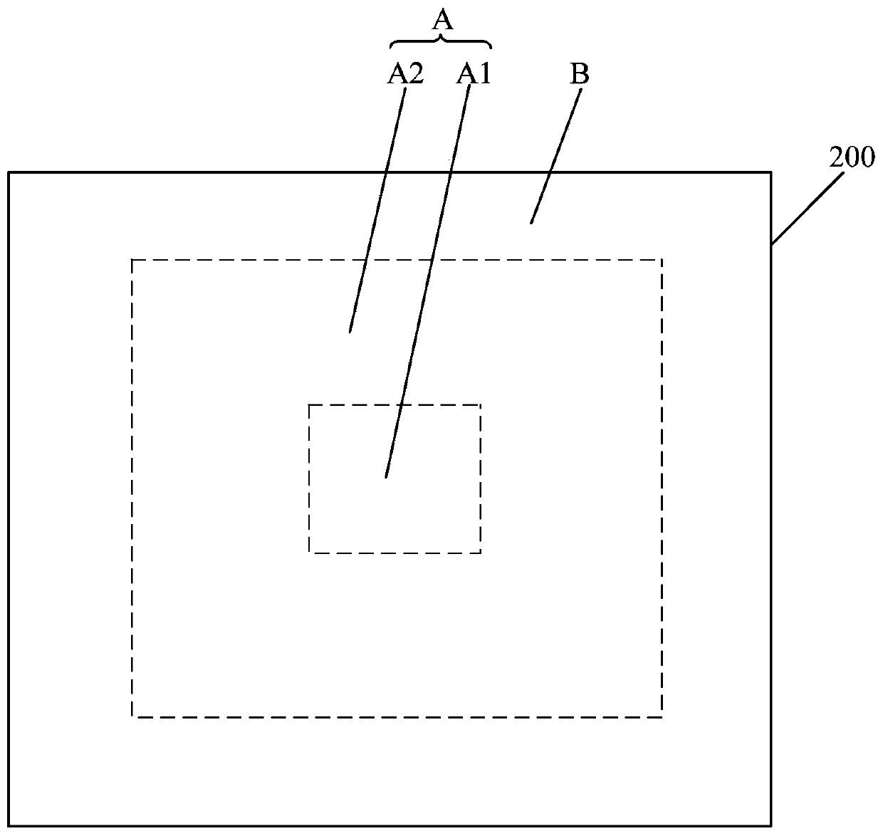
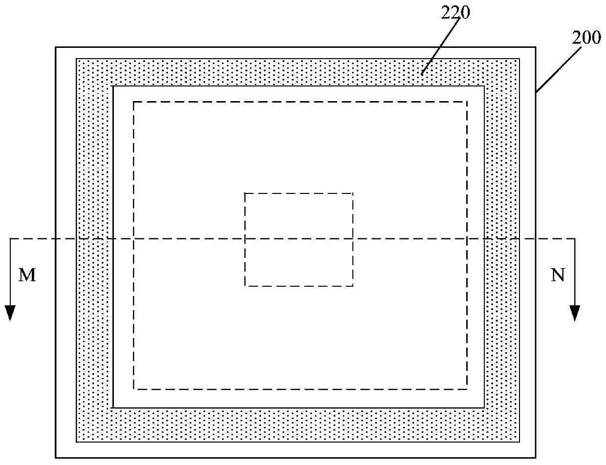
The invention discloses an image sensor, a forming method thereof and a camera module. The image sensor comprises a device substrate, a carrier substrate and a first piezoelectric structure, wherein the device substrate comprises a pixel area and an edge logic area which surrounds the pixel area; the carrier substrate is arranged to be opposite to the device substrate; the first piezoelectric structure is located between the edge logic area of the device substrate and the carrier substrate, surrounds the pixel area and is used for increasing the size in a first direction after obtaining a voltage signal; and the first direction is parallel to a normal direction on the surface of the center of the pixel area. The performance of the image sensor is improved.

Description

technical field [0001] The invention relates to the field of semiconductor manufacturing, in particular to an image sensor, a forming method thereof, and a camera module. Background technique [0002] With the development of semiconductor technology, image sensors have been widely used in various fields requiring digital imaging, such as digital cameras, digital video cameras and other electronic products. An image sensor is a semiconductor device that converts light signals into electrical signals. According to different photoelectric conversion methods, image sensors are classified into complementary metal oxide (CMOS) image sensors and charge-coupled device (CCD) image sensors. Among them, the CMOS image sensor has the advantages of simple process, easy integration of other devices, small size, light weight, low power consumption and low cost. Therefore, CMOS image sensors are easy to be integrated in portable electronic devices such as mobile phones, notebook computers...

Claims


Application Information

Patent Timeline
Patent Type & Authority Applications(China)
IPC IPC(8): H01L27/146H01L27/20H10N39/00
CPCH01L27/14609H01L27/14634H01L27/1469H10N39/00
Inventor 谢志峰
Owner ICLEAGUE TECH CO LTD
Learn More