Gene sequencing chip, equipment and manufacturing method
A technology of gene sequencing and manufacturing method, which is applied in the field of gene sequencing chip manufacturing, gene sequencing chip, and gene sequencing equipment, and can solve problems such as crosstalk of gene sequencing chips
- Summary
- Abstract
- Description
- Claims
- Application Information
AI Technical Summary
Problems solved by technology
Method used
Image
Examples
Embodiment 1
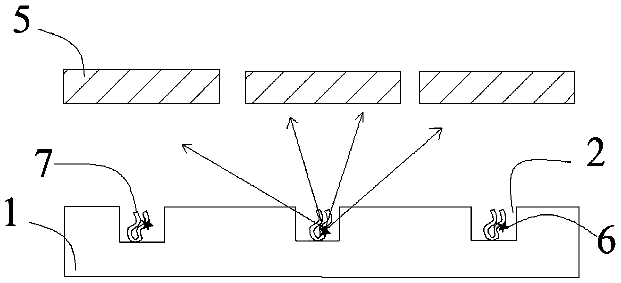
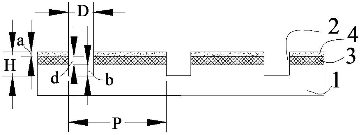
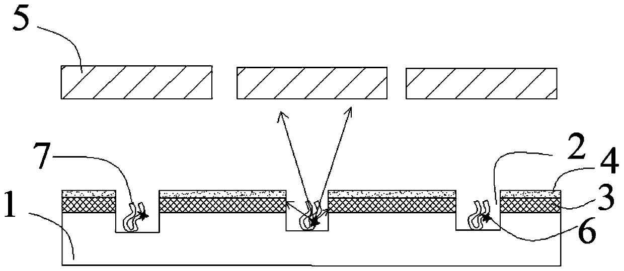
[0031] see Figure 2a and Figure 3a , this embodiment provides a gene sequencing chip, including a substrate 1 and a plurality of microporous structures 2 arranged on the substrate 1, and a light blocking structure 3 is arranged between adjacent microporous structures 2, and the light blocking structure 3 is used for The light emitted from the bottom of the microhole structure 2 is blocked from going to the detection unit 5 corresponding to the adjacent light blocking structure 3 .
[0032] The material of the substrate 1 is, for example, glass, silicon, or organic resin materials. The material of the base 1 of organic resin is, for example, polymethyl methacrylate (PMMA).
[0033] Such as Figure 2a As shown, the boundary of the microporous structure 2 may be formed on the substrate 1 and the light blocking structure 3 and the surface modification layer 4 on the substrate 1 . another example Figure 3a As shown, the boundaries of the microporous structure 2 are formed o...
Embodiment 2
[0050] This embodiment provides a gene sequencing device, including the gene sequencing chip of embodiment 1.
[0051] That is to say, the gene sequencing chip provided in Example 1 is applied to a gene sequencing device. Figure 2b and Figure 3b Only the detection unit 5 in the gene sequencing device is shown in . The parts except the gene sequencing chip can be configured according to the existing technology, so details will not be described here.
[0052] The gene sequencing equipment using the gene sequencing chip can effectively suppress or avoid the problem of crosstalk.
Embodiment 3
[0054] This embodiment provides a method for manufacturing a gene sequencing chip, comprising: a step of forming a plurality of microporous structures 2 on a substrate 1; a step of forming a light blocking structure 3 between adjacent microporous structures 2, the light blocking structure 3 is used to block the light emitted from the bottom of the microhole structure 2 from going to the detection unit 5 corresponding to the adjacent light blocking structure 3 . The gene sequencing chip prepared in this way can effectively avoid the problem of crosstalk.
[0055] Optionally, a step of forming a surface modification layer 4 covering the light blocking structure 3 is also included, wherein the surface modification layer 4 is used for receiving surface modification during gene sequencing. In this way, the reagent carrying the DNA molecule 7 can be combined with the surface modification layer 4 in subsequent applications to complete gene sequencing.
[0056] Two examples of specif...
PUM
 Abstract
Description
Claims
Application Information
 - R&D
- Intellectual Property
- Life Sciences
- Materials
- Tech Scout
- Unparalleled Data Quality
- Higher Quality Content
- 60% Fewer Hallucinations
Browse by: Latest US Patents, China's latest patents, Technical Efficacy Thesaurus, Application Domain, Technology Topic, Popular Technical Reports.
© 2025 PatSnap. All rights reserved.Legal|Privacy policy|Modern Slavery Act Transparency Statement|Sitemap|About US| Contact US: help@patsnap.com


