Structure and process method for preventing back scratching of glass substrate on dry-etched electrode surface

A glass substrate and electrode surface technology, which is applied to the coating process of metal materials, circuits, discharge tubes, etc., can solve problems such as glass scratches, pits, and product scrapping

Active Publication Date: 2021-08-03
芜湖通潮精密机械股份有限公司
View PDF3 Cites 0 Cited by
  • Summary
  • Abstract
  • Description
  • Claims
  • Application Information

AI Technical Summary

Problems solved by technology

At present, the dielectric layer on the surface of the lower electrode is Al 2 o 3 , the hardness is HV900±100, and the hardness of the glass substrate is HV600±50. Due to the increase of Coulomb force and plasma force, the high hardness dielectric layer will cause scratches and pits on the lower surface of the glass, resulting in product scrapping and a serious reduction Yield

Method used


Image

  • Structure and process method for preventing back scratching of glass substrate on dry-etched electrode surface
  • Structure and process method for preventing back scratching of glass substrate on dry-etched electrode surface

Examples


Embodiment 1

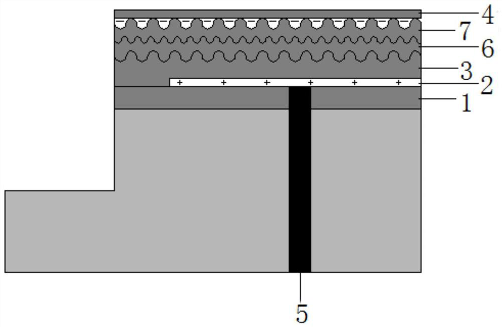
[0040] A process method for preventing the surface of the glass substrate surface of the dried electrode surface, the specific steps are as follows:

[0041] Step 1, cleaning drying: Wash the electrode using high pressure water, the deionized water resistance of the high pressure water is greater than 4mΩ * cm, the pressure is 100 bar, then the lower electrode surface is blown dry, and finally 60 ° C in the oven 24h.

[0042] Step 2, plasma spraying dense layers: Plasma spraying is Y 2 O 3 Alone 2 O 3 Composite powder, where Y 2 O 3 The content is at 80% (wt.), Plasma spraying, using a six-axis robot, the spray process parameter is: the main gas Ar flow 40L / min, the secondary h 2 The flow rate is 10 l / min, the voltage 36V, current 800a, and the amount of powder powder are 10 g / min, the spray distance is 100 mm, the thickness of the spray layer reaches 10 μm, and the bonding force reaches 10 MPa.

[0043] Step three, plasma spray top contact layer: Plasma spraying is Y 2 O 3 ...

Embodiment 2

[0048] A process method for preventing the surface of the glass substrate surface of the dried electrode surface, the specific steps are as follows:

[0049] Step 1, cleaning drying: Wash the electrode using high pressure water, the deionized water resistance rate of high pressure water is greater than 4mΩ * cm, the pressure is 150 bar, then the lower electrode surface is blown dry, and finally 80 ° C in the oven 12h.

[0050] Step 2, plasma spraying dense layers: Plasma spraying is Y 2 O 3 Alone 2 O 3 Composite powder, where Y 2 O 3 The content is 85% (wt.), Plasma spraying, using a six-axis robot, the spray process parameter is: the main gas Ar flow 60L / min, the secondary h 2 The flow rate is 15 l / min, the voltage is 40V, the current 900A, the amount of powder powder is 18 g / min, the spray distance is 150 mm, the spray coating has a thickness of 20 μm, and the bonding force reaches 10 MPa.

[0051] Step three, plasma spray top contact layer: Plasma spraying is Y 2 O 3 Alon...


PUM

PropertyMeasurementUnit
surface roughnessaaaaaaaaaa
electrical resistivityaaaaaaaaaa
thicknessaaaaaaaaaa

Abstract

The invention discloses a structure and a preparation method for preventing back scratching of a glass substrate on the surface of an electrode under dry etching. Floor. The present invention adds Y to the traditional lower electrode dielectric layer 2 o 3 and Al 2 o 3 Composite layer, control the surface hardness in the range of HV300~500, the coating hardness increases with Y 2 o 3 The content increases and decreases, so that the surface hardness of the lower electrode is lower than that of the glass, effectively preventing the occurrence of scratches and pits on the back of the glass.

Description

Technical field [0001] The present invention belongs to the field of dry carving electrode surface treatment, and in particular, the present invention relates to a structure in which the surface of the glass substrate surface of the dried lower electrode is to prevent the surface of the glass substrate. Background technique [0002] The engraving machine is a key device in the liquid crystal panel and the semiconductor preparation process. The lower electrode is a key component in the mutant machine, and the lower electricity is a typical sandwich structure. figure 1 Indicated. When the etching machine is working, the glass substrate is placed in the lower electrode surface, directly in contact with the lower electrode dielectric layer, and the DC power source is connected to the W layer through the down electrode back to the W layer, and the lower surface of the glass is generated. Negative charge Culen stress is generated between the positive charge and negative charge to adsor...

Claims


Application Information

Patent Timeline
Patent Type & Authority Patents(China)
IPC IPC(8): H01J37/305H01L21/3065C23C4/11G02F1/13C23C4/134
CPCC23C4/11C23C4/134G02F1/1303H01J37/3056H01L21/3065
Inventor 何新玉赵浩司奇峰
Owner 芜湖通潮精密机械股份有限公司
Why Eureka
Try Eureka