3D-stack CIS (CMOS Image Sensor) and bonding method thereof
A stacking and three-dimensional technology, which is applied in the field of three-dimensional stacking CIS and its bonding, can solve the problems of affecting the bonding effect and contact surface voids
- Summary
- Abstract
- Description
- Claims
- Application Information
AI Technical Summary
Problems solved by technology
Method used
Image
Examples
Embodiment Construction
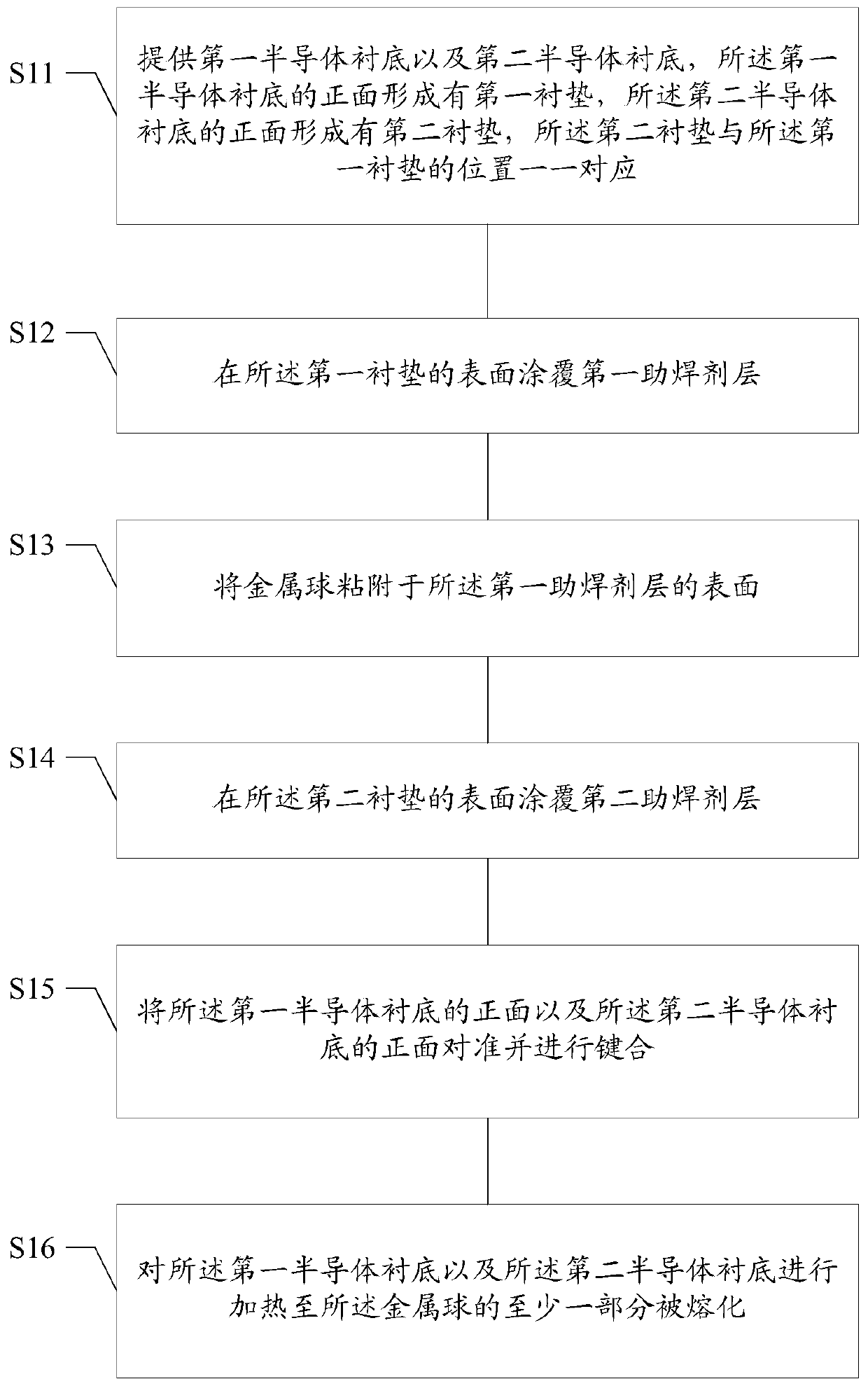
[0026] In the existing bonding process of the three-dimensional stacked CIS, two semiconductor substrates need to be bonded. Specifically, a logic device and a pixel device can be respectively formed in two semiconductor substrates, and then a flush copper pad is formed on the surface of the two semiconductor substrates by using a CMP process, and then a certain pressure is applied to the two semiconductor substrates. The substrates are bonded and interconnected between the copper pads.
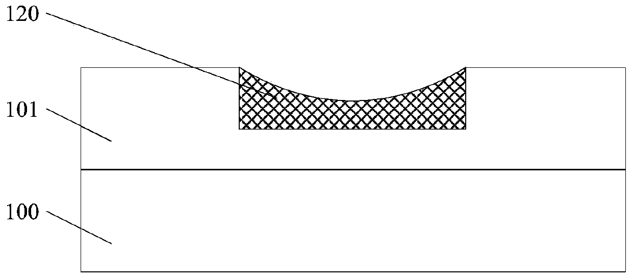
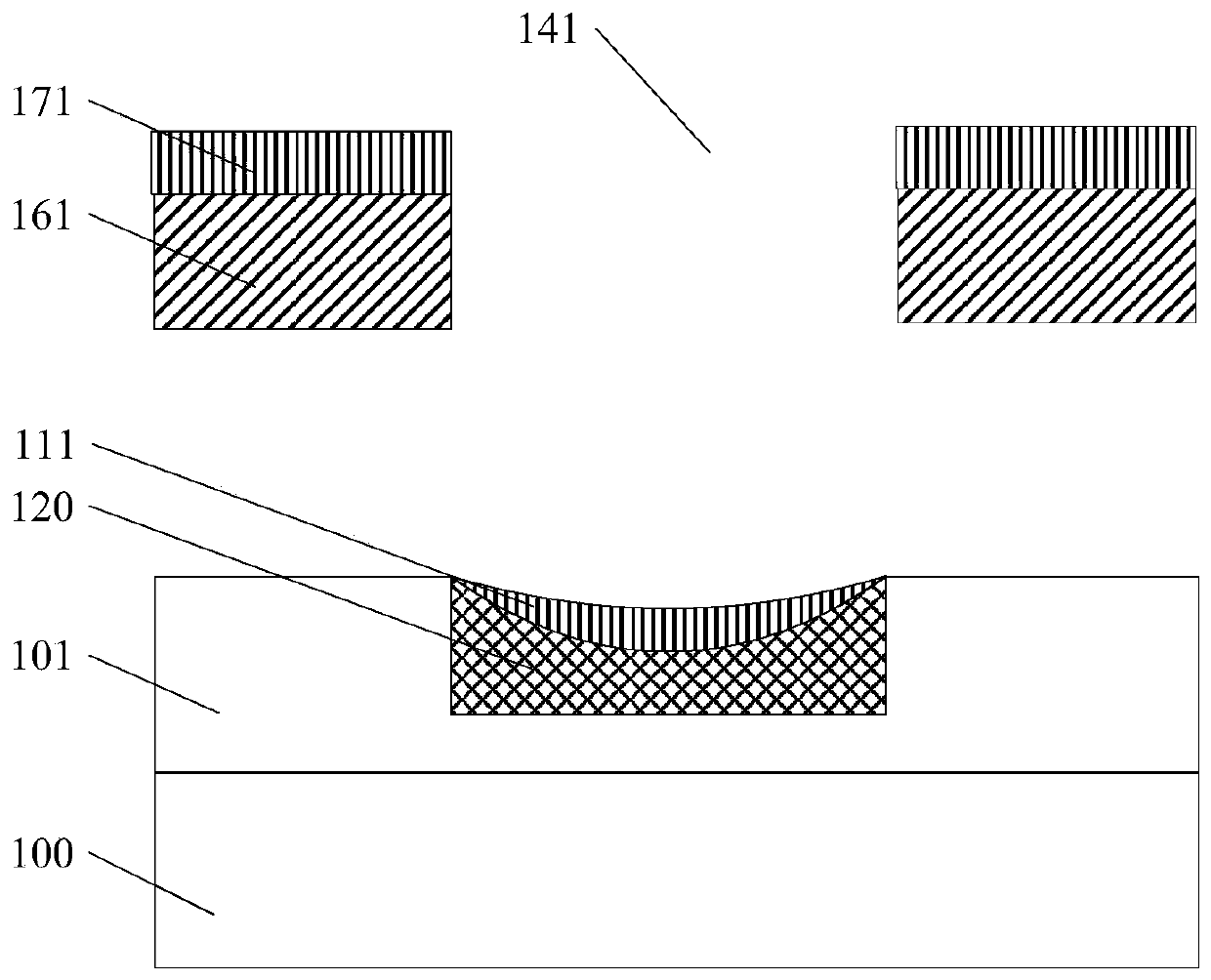
[0027] The inventors of the present invention have found through research that in the existing CMP process, there is a problem of grinding uniformity (Uniformity) due to the use of grinding fluid containing grinding particles for grinding. There are more abrasive particles and the grinding rate is higher, so after CMP, the surface of the copper pad will often have depressions. If the subsequent bonding pressure is not enough or the depression is too large, it will cause voids on the contact s...
PUM
 Abstract
Description
Claims
Application Information
 - Generate Ideas
- Intellectual Property
- Life Sciences
- Materials
- Tech Scout
- Unparalleled Data Quality
- Higher Quality Content
- 60% Fewer Hallucinations
Browse by: Latest US Patents, China's latest patents, Technical Efficacy Thesaurus, Application Domain, Technology Topic, Popular Technical Reports.
© 2025 PatSnap. All rights reserved.Legal|Privacy policy|Modern Slavery Act Transparency Statement|Sitemap|About US| Contact US: help@patsnap.com


