A kind of gallium oxide nano material transfer method
A technology of nanomaterials and transfer methods, which is applied in the field of separation of nanomaterials to achieve good separation effect, simple operation and high success rate of transfer
- Summary
- Abstract
- Description
- Claims
- Application Information
AI Technical Summary
Problems solved by technology
Method used
Image
Examples
Embodiment 1
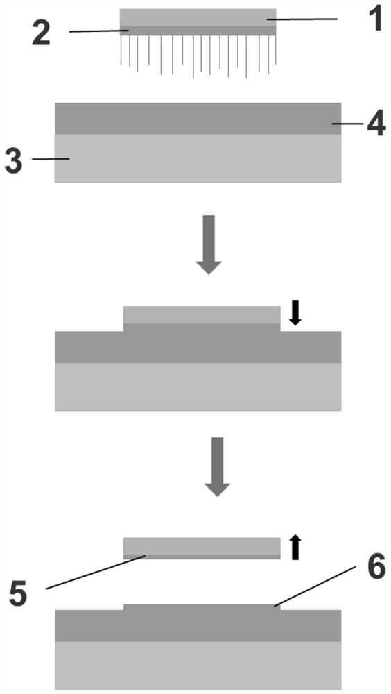
[0033] Example 1: Method for transferring gallium oxide nano.
[0034] The steps are as follows:
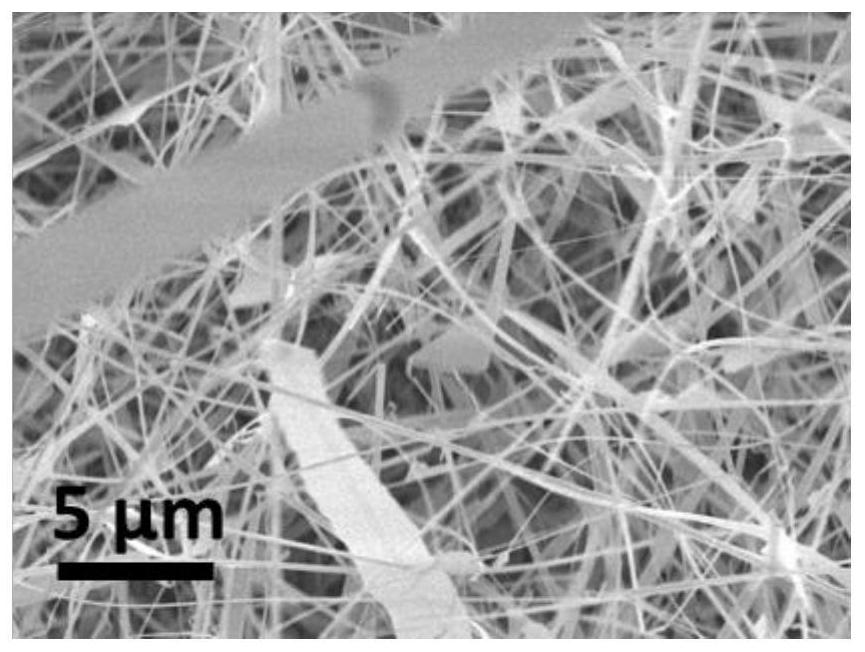
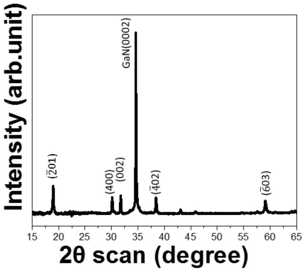
[0035] (1) A (0001) gallium nitride film is a substrate, an area of 2 mm × 2 mm, and a thickness of 20 μm, and a CVD method is generated on a gallium nitride film substrate to grow β-gallium oxide nanomaterials.
[0036] (2) Use polysilicon as a substrate material, deposit a layer of SiO on substrate material 2 The dielectric layer is to increase the adhesion between the gallium oxide material and the substrate and the insulation effect. SiO 2 The dielectric layer thickness is 200 nm.
[0037] (3) Put the growth of beta-gallium oxide nanomaterials, and use non-mechanical way to apply a specific force, that is, SiO 2 At 1cm height above the dielectric layer, the restriction is released, so that the β-gallium oxide nanomaterial layer naturally drops naturally due to gravity, bonded to SiO under the influence of gravity. 2 Medium layer.
[0038] (4) After the bonding, then the SIO 2 T...
Embodiment 2
[0040] Example 2: A method of transferring gallium oxide nanoji.
[0041] The steps are as follows:
[0042] (1) A (0001) gallium nitride film is a substrate, an area of 2 mm × 2 mm, and a thickness of 20 μm, and a CVD method is generated on a gallium nitride film substrate to grow β-gallium oxide nanomaterials.
[0043] (2) Use polysilicon as a substrate material, deposit a layer of SiO on substrate material 2 The dielectric layer is to increase the adhesion between the gallium oxide material and the substrate and the insulation effect. SiO 2 The dielectric layer thickness is 200 nm.
[0044] (3) The growth of the β-gallium oxide nanomaterial layer is facing downward, and the mechanical manner is applied, and the β-gallium oxide nanomaterial layer is placed in SiO. 2 On the dielectric layer, the β-gallium oxide nanomaterial layer was pressed using 0.1 N to press the β-gallium oxide nanomaterial layer in SiO. 2 Medium layer.
[0045] (4) After the bonding, then the SIO 2 The die...
Embodiment 3
[0049] Example 3: A method of transferring gallium oxide nanowires.
[0050] The steps are as follows:
[0051] (1) A (0001) gallium nitride film is a substrate, an area of 2 mm × 2 mm, and a thickness of 20 μm, and a CVD method is generated on a gallium nitride film substrate to grow β-gallium oxide nanomaterials.
[0052] (2) Use polysilicon as a substrate material, deposit a layer of SiO on substrate material 2 The dielectric layer is to increase the adhesion between the gallium oxide material and the substrate and the insulation effect. SiO 2The dielectric layer thickness is 200 nm.
[0053] (3) The growth of the β-gallium oxide nanomaterial layer is facing downward, and the mechanical manner is applied, and the β-gallium oxide nanomaterial layer is placed in SiO. 2 On the dielectric layer, the β-gallium oxide nanomaterial layer was pressed using 0.1 N to press the β-gallium oxide nanomaterial layer in SiO. 2 Medium layer.
[0054] (4) After the bonding, then the SIO 2 The d...
PUM
| Property | Measurement | Unit |
|---|---|---|
| thickness | aaaaa | aaaaa |
Abstract
Description
Claims
Application Information
 - R&D
- Intellectual Property
- Life Sciences
- Materials
- Tech Scout
- Unparalleled Data Quality
- Higher Quality Content
- 60% Fewer Hallucinations
Browse by: Latest US Patents, China's latest patents, Technical Efficacy Thesaurus, Application Domain, Technology Topic, Popular Technical Reports.
© 2025 PatSnap. All rights reserved.Legal|Privacy policy|Modern Slavery Act Transparency Statement|Sitemap|About US| Contact US: help@patsnap.com


