Two-dimensional-arrangement double-sided staggered embedded type three-dimensional detector and preparation method and array thereof

A two-dimensional arrangement and detector technology, applied in semiconductor devices, final product manufacturing, radiation control devices, etc., can solve the problems of easy breakdown position resolution, the number of electronic readout channels, and the complexity of electronics, etc. Achieve the effects of reduced risk of breakdown, uniform electric field distribution, and improved position resolution

Pending Publication Date: 2019-06-25
XIANGTAN UNIV
View PDF0 Cites 0 Cited by
  • Summary
  • Abstract
  • Description
  • Claims
  • Application Information

AI Technical Summary

Problems solved by technology

[0004] The object of the present invention is to provide a two-dimensional arrangement double-sided interlaced three-dimensional detector and its preparation method and array, which solves the problem of low sensitivity of the existing three-dimensional groove electrode detector and the large number of electronic read-out channels resulting in complicated electronics. , easy to be broken down and low position resolution

Method used


Image

  • Two-dimensional-arrangement double-sided staggered embedded type three-dimensional detector and preparation method and array thereof
  • Two-dimensional-arrangement double-sided staggered embedded type three-dimensional detector and preparation method and array thereof
  • Two-dimensional-arrangement double-sided staggered embedded type three-dimensional detector and preparation method and array thereof

Examples


Embodiment 1

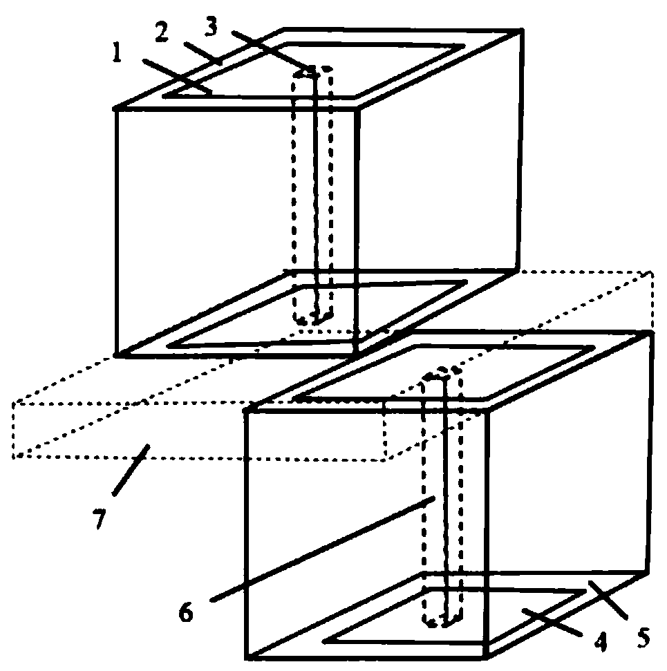
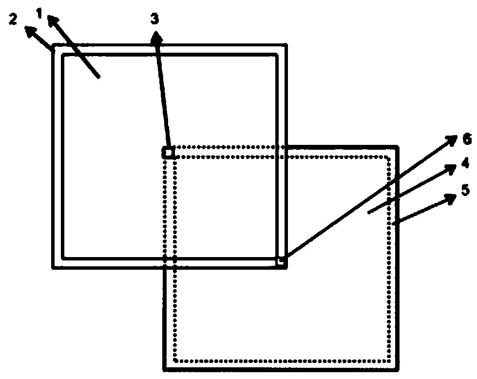
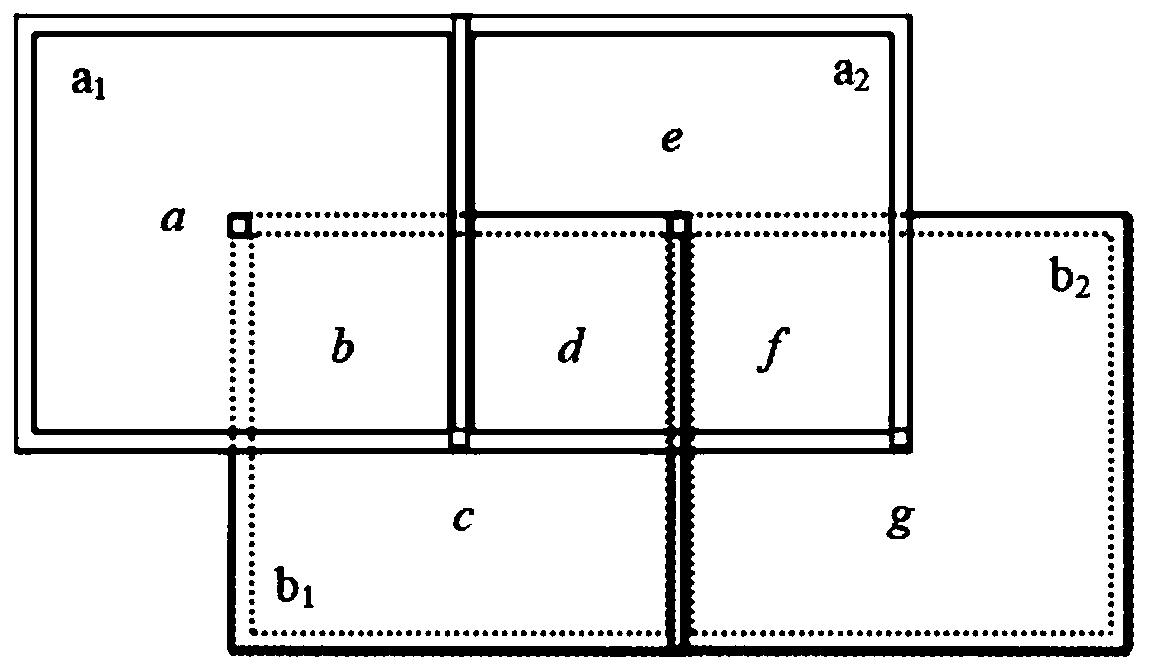
[0033] Two-dimensional arrangement of double-sided staggered three-dimensional detectors, such as Figure 1~3 As shown, the third silicon base 7 is included, the upper surface of the third silicon base 7 is etched with the upper trench electrode 2, the lower surface of the third silicon base 7 is etched with the lower trench electrode 5, the upper trench electrode 2 and the lower trench The groove electrode 5 is a hollow cuboid structure, the upper groove electrode 2 is embedded with the upper central electrode 3, the lower groove electrode 5 is embedded with the lower central electrode 6, and the gap between the upper central electrode 3 and the upper groove electrode 2 is filled with The lower semiconductor base 4 is filled between the upper semiconductor base 1 , the lower trench electrode 5 and the lower central electrode 6 . The outer length of the upper trench electrode 2 is 2R X , the outer width is 2R Y , the vertical distance between the centers of the upper central...

Embodiment 2

[0035] The difference from embodiment 1 is that the upper trench electrode 2 and the lower trench electrode 5 in this embodiment have a doping concentration of 25×10 18 cm -3 The p-type heavily doped silicon substrate; the upper central electrode 3 and the lower central electrode 6 have a doping concentration of 25×10 18 cm -3 n-type heavily doped silicon substrate.

Embodiment 3

[0037] The difference from Examples 1-2 is that the upper trench electrode 2 and the lower trench electrode 5 in this example have a doping concentration of 5×10 19 cm -3 The p-type heavily doped silicon substrate; the upper central electrode 3 and the lower central electrode 6 have a doping concentration of 5×10 19 cm -3 n-type heavily doped silicon substrate.


PUM


Abstract

The invention discloses a two-dimensional-arrangement double-sided staggered embedded type three-dimensional detector and a preparation method and array thereof. The detector comprises an upper trenchelectrode and a lower trench electrode, wherein the upper trench electrode and the lower trench electrode are etched on the surface of an intermediate semiconductor substrate; an upper central electrode is embedded in the upper groove electrode, and an upper semiconductor substrate is filled between the upper central electrode and the upper groove electrode; a lower central electrode is embeddedin the lower groove electrode, and a lower semiconductor substrate is filled between the lower groove electrode and the lower central electrode; the outer widths of the upper trench electrode and thelower trench electrode are 2RX; the lower trench electrode is located below the upper trench electrode, and the vertical distance d3 is formed between the upper trench electrode and the lower trench electrode; 1/4 of parts of the upper trench electrode and the lower trench electrode are overlapped, and the upper central electrode and the lower central electrode are of the same specification. A silicon dioxide layer is generated on the surface of a chip through gettering oxidation, a detector pattern is transferred to the silicon dioxide layer through marking and photoetching, etching and chemical deposition diffusion of a cathode electrode and an anode electrode are carried out, and finally damage repair and packaging are carried out.

Description

technical field [0001] The invention belongs to the technical field of photons (including X-rays, lasers, and X-ray free electron lasers) or particle detection, and relates to a two-dimensionally arranged double-sided staggered-embedded three-dimensional detector, a preparation method and an array thereof. Background technique [0002] The three-dimensional trench electrode silicon detector is to etch a certain depth of trench electrodes and central electrodes on one side of the chip. If the trench electrodes are etched through the chip to form a loop, the detector will fall between the chips. outside. Therefore, the groove electrode and the central electrode with a certain depth (less than the chip depth) are etched on one side of the chip, and the bottom not surrounded by the groove electrode is a dead zone, and the depth of the bottom dead zone is the same as that of the groove electrode etched on one side. The sum of the etching depths is the total depth of the chip. T...

Claims


Application Information

Patent Timeline
Patent Type & Authority Applications(China)
IPC IPC(8): H01L31/0224H01L31/101H01L27/144H01L31/18
CPCY02P70/50
Inventor 李正张亚
Owner XIANGTAN UNIV
Why Eureka
Try Eureka