RRAM device based on graphene oxide and preparation method of RRAM device

A graphene and device technology, applied in the field of graphene oxide-based RRAM devices and its preparation, can solve problems such as high production costs, limited equipment, and inability to meet the needs of large-scale and low-cost industrialization, and achieve resistive switching effects Good, less investment in equipment and raw materials, and achieve the effect of large-scale industrial application

Pending Publication Date: 2019-06-07
XIAN JIAOTONG LIVERPOOL UNIV
View PDF6 Cites 1 Cited by
  • Summary
  • Abstract
  • Description
  • Claims
  • Application Information

AI Technical Summary

Problems solved by technology

[0003] The existing preparation processes for RRAM dielectric layers are relatively traditional, such as magnetron radio frequency sputtering, chemical vapor deposition (CVD), atomic layer deposition (ALD), etc., but the above methods are limited by equipment, high production costs, and cannot Meet the needs of large-scale and low-cost industrialization

Method used


Image

  • RRAM device based on graphene oxide and preparation method of RRAM device
  • RRAM device based on graphene oxide and preparation method of RRAM device

Examples


Embodiment 1

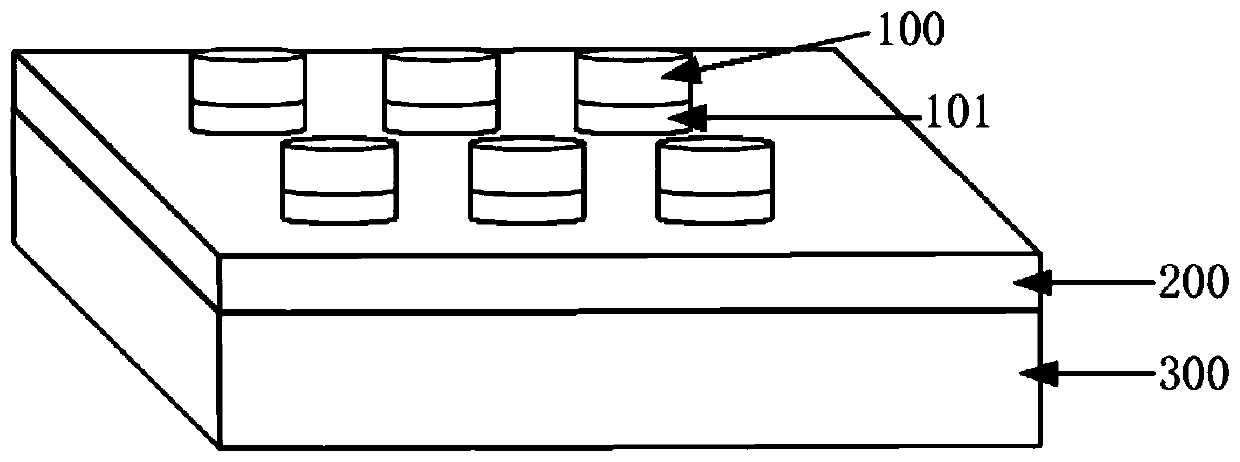
[0033] like figure 1 As shown, this embodiment relates to a graphene oxide-based RRAM device, including a conductive substrate 300, a dielectric layer 200, and a top electrode layer stacked from bottom to top, and the top electrode layer includes several top electrodes arrayed on the dielectric layer 200 101 , the top electrode 101 is provided with a protective layer 100 on the surface away from the dielectric layer 200 .

[0034] The protective layer 100 adopts metal tungsten thin film.

[0035] The top electrode 101 is a cylindrical metal aluminum film with a thickness of 30-80 nm and a diameter of 0.1-0.3 mm, preferably a thickness of 40 nm and a diameter of 0.1 mm.

[0036] The dielectric layer 200 is a graphene oxide film with a thickness of 20-80 nm.

[0037] The conductive substrate 300 adopts a highly doped silicon film with a thickness of 50-150 nm, preferably, an N-type phosphorous-doped highly doped silicon film with a thickness of 100 nm.

[0038] This embodimen...


PUM

PropertyMeasurementUnit
Thicknessaaaaaaaaaa
Diameteraaaaaaaaaa
Thicknessaaaaaaaaaa

Abstract

The invention discloses an RRAM device based on graphene oxide and a preparation method of the RRAM device, and belongs to the technical field of electronic devices. The RRAM device based on the graphene oxide comprises a conductive substrate, a dielectric layer and a top electrode layer, which are stacked from bottom to top. The top electrode layer comprises a plurality of top electrodes arrangedon the dielectric layer in an array mode, and a protective layer is arranged on the surfaces, away from the dielectric layer, of the top electrodes. The dielectric layer is manufactured through a solution method, the low-cost preparation of the RRAM device is realized, the equipment and raw material investment is less, and the large-scale industrial application can be realized.

Description

technical field [0001] The present invention relates to a technology in the field of electronic devices, in particular to a graphene oxide-based RRAM device (Resistive random access memory, resistive random access memory) and a preparation method thereof. Background technique [0002] The rapid development of information puts forward higher requirements for information storage and logic circuits. Due to the low storage density, high processing cost, complex device manufacturing process, and material limitations, the traditional memory based on metal oxide materials has reached its development limit, and can no longer meet the needs of the rapid development of information storage. Graphene and its oxides as storage materials can provide better mechanical flexibility, faster response time, higher switching ratio, etc., and can realize the miniaturization of circuits. [0003] The existing preparation processes for RRAM dielectric layers are relatively traditional, such as mag...

Claims


Application Information

Patent Timeline
IPC IPC(8): H01L45/00
Inventor 沈棕杰赵春赵策洲杨莉张艺罗天黄彦博
Owner XIAN JIAOTONG LIVERPOOL UNIV
Why Eureka
Try Eureka