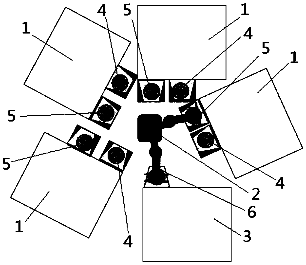
Silicon wafer CMP post-processing equipment and processing flow
A silicon wafer and equipment technology, which is applied in the field of silicon wafer CMP post-processing equipment and processing flow, can solve the problems of high worker intensity, low productivity, and incomplete cleaning effect, and achieve high cleaning precision and high productivity.
- Summary
- Abstract
- Description
- Claims
- Application Information
AI Technical Summary
Problems solved by technology
Method used
Image


Examples
Embodiment 1
[0067] Embodiment one: a kind of cleaning process after silicon chip CMP, comprises the following steps:
[0068] (1) Pre-cleaning:
[0069] Step1: Carry out vibration cleaning to silicon chip by ozone water and ultrasonic cleaning equipment for 20 seconds;
[0070] Step2: first utilize the hydrofluoric acid of concentration 2% to rinse the silicon wafer for 10 seconds, then utilize ozone water to rinse the silicon wafer for 30 seconds;
[0071] Step3: Repeat the operation of Step2 three times, and alternately rinse the silicon wafer with hydrofluoric acid and ozone water several times;
[0072] Step4: Brush the front side of the silicon wafer with the alkaline liquid medicine, and the scrubbing time is 2 minutes;
[0073] Step5: Rinse the silicon wafer with pure water for 10 seconds, and finally spin the silicon wafer to dry.
[0074] (2) Inspection, use the inspection machine to inspect the pre-cleaned silicon wafers, if the pre-cleaned silicon wafers meet the requirement...
Embodiment 2
[0080] A cleaning process after silicon chip CMP comprises the steps:
[0081] (1) Pre-cleaning:
[0082] Step1: Carry out vibratory cleaning to silicon chip by ozone water and ultrasonic cleaning equipment for 80 seconds;
[0083] Step2: first utilize the hydrofluoric acid of concentration 4% to rinse the silicon wafer for 18 seconds, then utilize ozone water to rinse the silicon wafer for 36 seconds;
[0084] Step3: Repeat the operation of Step2 5 times, and alternately rinse the silicon wafer with hydrofluoric acid and ozone water several times;
[0085] Step4: Brush the front of the silicon wafer with the alkaline liquid medicine, and the scrubbing time is 4 minutes;
[0086] Step5: Rinse the silicon wafer with pure water for 50 seconds, and finally spin the silicon wafer to dry.
[0087] (2) Inspection, use the inspection machine to inspect the pre-cleaned silicon wafers, if the pre-cleaned silicon wafers meet the requirements, enter step three; if not meet the require...
Embodiment 3
[0092] Embodiment three: a kind of cleaning process after silicon chip CMP, comprises the following steps:
[0093] (1) Pre-cleaning:
[0094] Step1: Carry out vibratory cleaning to silicon chip by ozone water and ultrasonic cleaning equipment for 30 seconds;
[0095] Step2: first utilize the hydrofluoric acid of concentration 1.5% to rinse the silicon wafer for 10 seconds, and then utilize ozone water to rinse the silicon wafer for 33 seconds;
[0096] Step3: Repeat the operation of Step2 three times, and alternately rinse the silicon wafer with hydrofluoric acid and ozone water several times;
[0097] Step4: Brush the front side of the silicon wafer with the alkaline liquid medicine, and the scrubbing time is 1.5 minutes;
[0098] Step5: Rinse the silicon wafer with pure water for 12 seconds, and finally spin and dry the silicon wafer.
[0099] (2) Inspection, use the inspection machine to inspect the pre-cleaned silicon wafers, if the pre-cleaned silicon wafers meet the ...
PUM
 Abstract
Description
Claims
Application Information
 - Generate Ideas
- Intellectual Property
- Life Sciences
- Materials
- Tech Scout
- Unparalleled Data Quality
- Higher Quality Content
- 60% Fewer Hallucinations
Browse by: Latest US Patents, China's latest patents, Technical Efficacy Thesaurus, Application Domain, Technology Topic, Popular Technical Reports.
© 2025 PatSnap. All rights reserved.Legal|Privacy policy|Modern Slavery Act Transparency Statement|Sitemap|About US| Contact US: help@patsnap.com