High-quality semi-polar two-dimensional ultra-thin indium nitrogen/gallium nitride laminated structure and preparation method thereof
A stacked structure, semi-polar technology, applied in semiconductor/solid-state device manufacturing, semiconductor devices, semiconductor lasers, etc., can solve problems such as large stress, limited theoretical research results, etc.
- Summary
- Abstract
- Description
- Claims
- Application Information
AI Technical Summary
Problems solved by technology
Method used
Image
Examples
preparation example Construction
[0067] This embodiment provides a method for preparing a high-quality semipolar {11-22} two-dimensional ultra-thin indium nitride / gallium nitride stack structure, the steps are as follows:
[0068] (1) growing semipolar {11-22} gallium nitride thin films on the substrate;
[0069] (2) In the reaction chamber, a periodic two-dimensional ultra-thin indium nitride / gallium nitride stack structure is grown on the semipolar {11-22} gallium nitride film.
[0070] The growth process of the two-dimensional ultra-thin InN / GaN stack structure is:
[0071] growing an indium nitride layer;
[0072] Grow a thin layer of gallium nitride at the same growth temperature as the indium nitride layer;
[0073] GaN barrier layer is grown.
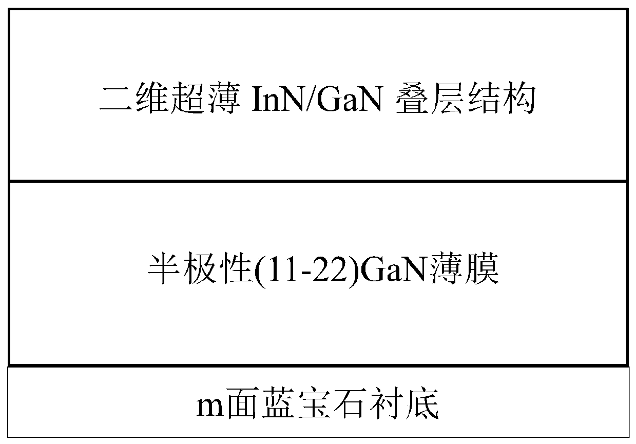
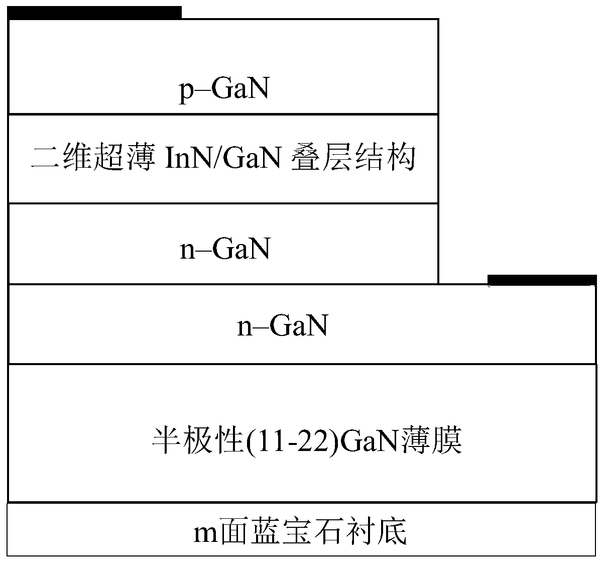
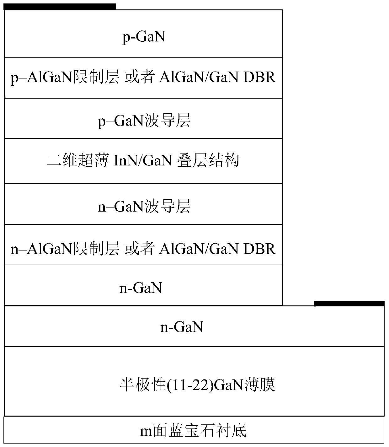
[0074] This embodiment also provides a high-quality semipolar {11-22} two-dimensional ultra-thin indium nitride / gallium nitride stack structure, such as figure 1 As shown, it includes a substrate, a semipolar gallium nitride film, and a two-dimensional ultra...
Embodiment 1
[0076] Example 1: High-quality semipolar {11-22} two-dimensional ultra-thin indium nitride / gallium nitride stacked structure
[0077] (1) growing semipolar {11-22} gallium nitride thin films on the substrate;
[0078] (2) A 20-period two-dimensional ultrathin indium nitride / gallium nitride stack structure was grown on the prepared semipolar {11-22} gallium nitride film;
[0079] The growth parameters of the two-dimensional ultrathin InN / GaN stack structure are as follows:
[0080] The pressure in the reaction chamber is in the range of 300Torr, and the two-dimensional ultra-thin indium nitride / gallium nitride stack structure is grown;
[0081] Indium nitrogen layer: the substrate temperature is 680° C.; the thickness of the indium nitrogen layer is ~1 nm.
[0082] Subsequently, before growing the gallium nitride barrier layer, a thin layer of gallium nitride is grown as a protective layer of indium nitrogen, the growth temperature is the same as that of the indium nitride la...
Embodiment 2
[0085] Example 2: High-quality semipolar {11-22} two-dimensional ultra-thin indium nitride / gallium nitride stacked structure
[0086] (1) growing semipolar {11-22} gallium nitride thin films on the substrate;
[0087] (2) A 30-period two-dimensional ultrathin indium nitride / gallium nitride stack structure was grown on the prepared semipolar {11-22} gallium nitride film;
[0088] The growth parameters of the two-dimensional ultrathin InN / GaN stack structure are as follows:
[0089] The pressure in the reaction chamber is in the range of 300Torr, and the two-dimensional ultra-thin indium nitride / gallium nitride stack structure is grown;
[0090] Indium nitrogen layer: the substrate temperature is 680° C.; the thickness of the indium nitrogen layer is ~0.6 nm.
[0091] Subsequently, before growing the gallium nitride barrier layer, a thin layer of gallium nitride is grown as a protective layer of indium nitrogen, the growth temperature is the same as that of the indium nitride ...
PUM
| Property | Measurement | Unit |
|---|---|---|
| thickness | aaaaa | aaaaa |
| thickness | aaaaa | aaaaa |
| thickness | aaaaa | aaaaa |
Abstract
Description
Claims
Application Information
 - R&D Engineer
- R&D Manager
- IP Professional
- Industry Leading Data Capabilities
- Powerful AI technology
- Patent DNA Extraction
Browse by: Latest US Patents, China's latest patents, Technical Efficacy Thesaurus, Application Domain, Technology Topic, Popular Technical Reports.
© 2024 PatSnap. All rights reserved.Legal|Privacy policy|Modern Slavery Act Transparency Statement|Sitemap|About US| Contact US: help@patsnap.com


