Silicon crystal orientation discriminator

A discriminator and silicon crystal technology, which is applied in the field of optics, can solve the problems of limited positioning accuracy of the notch in the wafer crystal direction, cannot meet the processing requirements of micro devices, and the quality of processed products is not high, and achieve simple structure, high reliability, and fast response fast effect

Active Publication Date: 2021-08-13
UNIV OF SHANGHAI FOR SCI & TECH
View PDF4 Cites 0 Cited by
  • Summary
  • Abstract
  • Description
  • Claims
  • Application Information

AI Technical Summary

Problems solved by technology

However, in the actual production of micro-devices, the positioning accuracy of the notch of the wafer is limited, which cannot meet the processing requirements of micro-devices, and in the process of micro-devices, due to the existence of this alignment error low quality
Especially for those micro devices with slender rod structure, the error is larger

Method used


Image

  • Silicon crystal orientation discriminator

Examples


Embodiment Construction

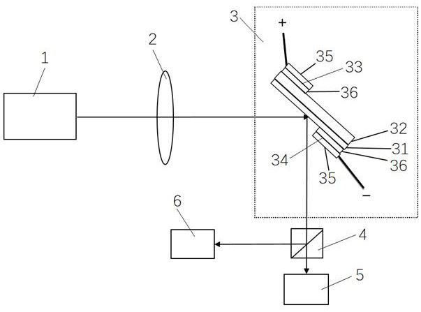
[0012] Example figure 1 As shown, the silicon crystal orientation discriminator of the present invention includes a laser emitter 1, a lens 2, a detection unit 3, a beam splitting unit 4, a light intensity detector 5, and a polarization detector 6 arranged sequentially along the beam direction, and the laser emitter 1. The emitted laser light is focused by the lens 2 and irradiated to the detection unit 3. The detection unit 3 forms reflected light and outputs it to the beam splitting unit 4. The beam splitting unit 4 outputs two beams and is respectively detected by the light intensity. Receiver 5 and polarization detector 6, the light intensity detector 5 measures the light intensity and spot displacement of the reflected laser light after the detection unit 3, and the polarization detector 6 measures the polarization of the reflected laser light after the inspection unit 3 and spot displacement.

[0013] Preferably, the detection unit 3 includes a silicon plate 32 coated w...


PUM

PropertyMeasurementUnit
thicknessaaaaaaaaaa
thicknessaaaaaaaaaa
thicknessaaaaaaaaaa

Abstract

The invention discloses a silicon crystal orientation discriminator. The discriminator comprises a laser emitter, a lens, a detection unit, a beam splitting unit, a light intensity detector and a polarization detector arranged sequentially along the beam direction. The laser emitted by the laser emitter After being focused by the lens, it is irradiated to the detection unit. The detection unit forms reflected light and outputs it to the beam splitting unit. The beam splitting unit outputs two beams and is respectively received by the light intensity detector and the polarization detector. The light intensity of the reflected laser light and the displacement of the light spot, the polarization detector measures the polarization of the reflected laser light and the displacement of the light spot after passing through the inspection unit. This discriminator effectively improves the accuracy of silicon crystal direction identification, thereby improving the alignment accuracy of the mask plate and the large crystal direction of the wafer, and the structure of the optical path components is simple, reducing equipment costs, and has the advantages of fast response, high precision, and high reliability. .

Description

technical field [0001] The invention relates to the field of optical technology, in particular to a silicon crystal orientation discriminator. Background technique [0002] At present, the traditional methods for identifying the crystal orientation of silicon are mostly X-ray diffraction crystal orientation calibration technology and laser reflection calibration method, but the required equipment is expensive and the accuracy is not high. In the processing of micro-devices, the anisotropic etching characteristics of single crystal silicon materials are used to form structures of various shapes by wet chemical processes. In this processing technology, the alignment accuracy of the pattern on the mask plate and the large crystal direction of the wafer has a great influence on the manufacturing accuracy of the unprocessed micro-devices. Therefore, it is the key technology of this processing technology to make the direction of the mask plate accurately locate to the specified c...

Claims


Application Information

Patent Timeline
Patent Type & Authority Patents(China)
IPC IPC(8): G01N21/84G01N21/21G01N21/47
Inventor 王振宇乔治蔡一博高文强沈世华焦新兵
Owner UNIV OF SHANGHAI FOR SCI & TECH
Why Eureka
Try Eureka