
A method for preparing an electronic circuit on a substrate

A technology of electronic circuits and substrates, applied in the field of electrochemical processing, can solve problems such as circuit short circuit and abnormal production, and achieve the effect of improving the overflow plating situation and avoiding the overflow plating phenomenon

Active Publication Date: 2021-10-22
SHANGHAI AMPHENOL AIRWAVE COMM ELECTRONICS CO LTD
View PDF4 Cites 0 Cited by
  • Summary
  • Abstract
  • Description
  • Claims
  • Application Information

AI Technical Summary

Problems solved by technology

[0003] In the usual electroless plating process, the gap (gap) between each line must be at least 0.3mm in order to ensure the quality of electroless plating and avoid the short circuit of the line due to overflow plating. At present, there are more and more small gap requirements. At present The LDS and electroless plating methods cannot be produced normally. For the case where the gap is less than 0.3mm, there are often circuit short circuits.

Method used


Image

  • A method for preparing an electronic circuit on a substrate
  • A method for preparing an electronic circuit on a substrate
  • A method for preparing an electronic circuit on a substrate

Examples


Embodiment 1

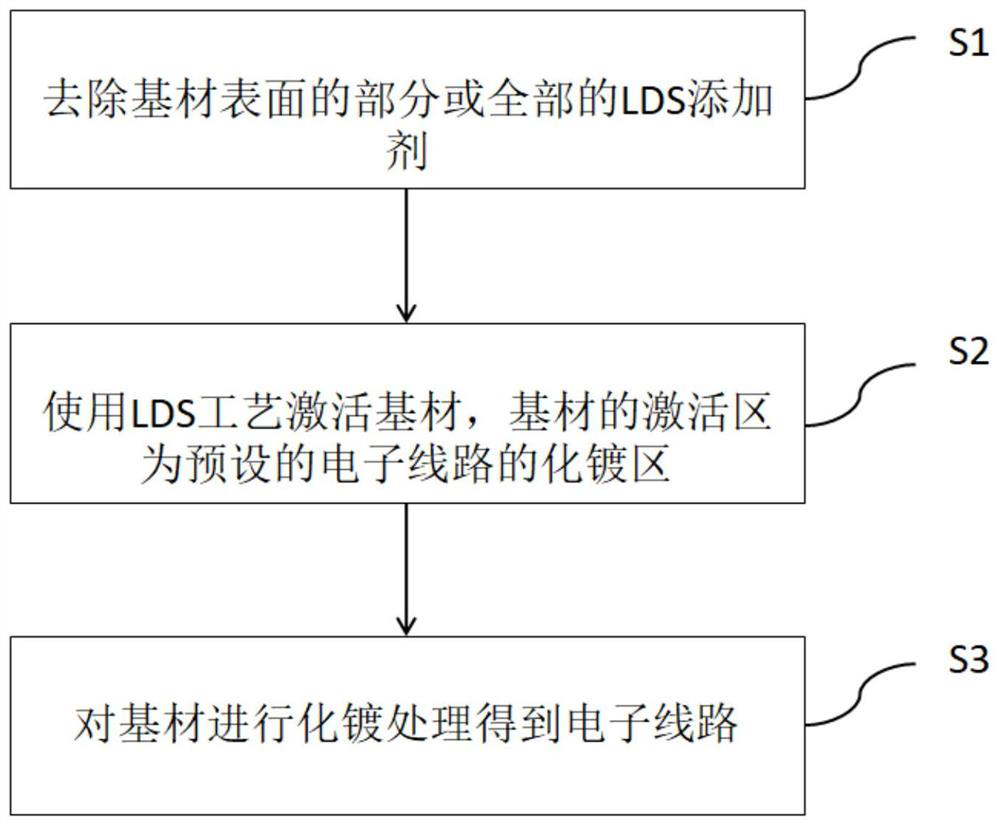
[0032] see figure 1 , a method for preparing an electronic circuit 2 on a substrate 1, comprising:

[0033] S1, removing part or all of the LDS additive on the surface of the substrate 1;

[0034] S2, using the LDS process to activate the substrate 1, the activation area of ​​the substrate 1 is the preset electroless plating area of ​​the electronic circuit 2;

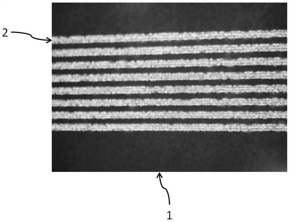
[0035] S3, performing electroless plating treatment on the substrate 1 to obtain the electronic circuit 2 . For the product structure prepared in this step, see figure 2 .

[0036] The substrate 1 in this embodiment can be a plastic material containing metal elements, and the metal elements usually exist in the form of compounds (LDS additives). The metal particles are based on the metal particles during the electroless plating, and a metal plating layer will be formed in the area irradiated by the laser (the preset electroless plating area of ​​the electronic circuit 2 ) to form the electronic circuit 2 .

[003...

Embodiment 2

[0048] see Figure 8 , a method for preparing an electronic circuit 2 on a substrate 1, comprising:

[0049] B1, injecting glass fiber into the base material 1, the direction of the glass fiber is consistent with the direction of the preset electronic circuit 2;

[0050] B2, removing part or all of the LDS additive on the surface of the substrate 1;

[0051] B3, using the LDS process to activate the substrate 1, the activation area of ​​the substrate 1 is the preset electroless plating area of ​​the electronic circuit 2;

[0052] B4, performing electroless plating treatment on the base material 1 to obtain the electronic circuit 2 . For the product structure prepared in this step, see figure 2 .

[0053] The substrate 1 in this embodiment can be a plastic material containing metal elements, and the metal elements usually exist in the form of compounds (LDS additives). The metal particles are based on the metal particles during the electroless plating, and a metal plating...


PUM


Abstract

The invention discloses a method for preparing an electronic circuit on a base material, comprising: S1, removing part or all of the LDS additive on the surface of the base material; S2, activating the base material by using an LDS process, and the activation area of ​​the base material is preset The electroless plating area of ​​the electronic circuit; S3, performing electroless plating on the base material to obtain the electronic circuit. The method for preparing an electronic circuit can avoid overflow plating phenomenon in the prepared electronic circuit with small pitch.

Description

technical field [0001] The invention belongs to the technical field of electrochemical processing, in particular to a method for preparing electronic circuits on a base material. Background technique [0002] In current electronic products, after the circuit substrate is processed by LDS (Laser Direct Structuring, laser direct structuring technology), electroless plating is used to deposit a metal coating on the surface of the substrate to form a circuit. [0003] In the usual electroless plating process, the gap (gap) between each line must be at least 0.3mm in order to ensure the quality of electroless plating and avoid the short circuit of the line due to overflow plating. At present, there are more and more small gap requirements. At present The LDS and electroless plating methods cannot be produced normally. For the case where the gap is less than 0.3mm, the circuit often short-circuits. Contents of the invention [0004] The technical purpose of the present inventio...

Claims


Application Information

Patent Timeline
Patent Type & Authority Patents(China)
IPC IPC(8): H05K3/18
Inventor 马承文徐映伟翟后明张文宇张东胜苏娅
Owner SHANGHAI AMPHENOL AIRWAVE COMM ELECTRONICS CO LTD
Learn More