
A design drawing editing method of a CPU in a PCB and a related device

A PCB board and design drawing technology, applied in the field of computer-readable storage media, can solve problems such as product quality risks and damage

Active Publication Date: 2019-05-10
ZHENGZHOU YUNHAI INFORMATION TECH CO LTD
View PDF7 Cites 0 Cited by
  • Summary
  • Abstract
  • Description
  • Claims
  • Application Information

AI Technical Summary

Problems solved by technology

If the alignment is inaccurate, it will cause damage to the CPU during loading and unloading, which will put the product quality at risk

Method used


Image

  • A design drawing editing method of a CPU in a PCB and a related device
  • A design drawing editing method of a CPU in a PCB and a related device
  • A design drawing editing method of a CPU in a PCB and a related device

Examples


Embodiment Construction

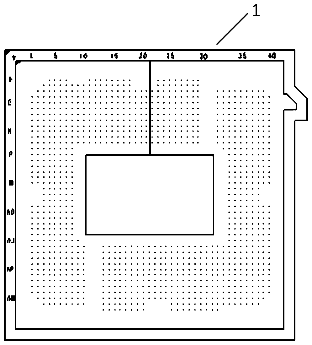
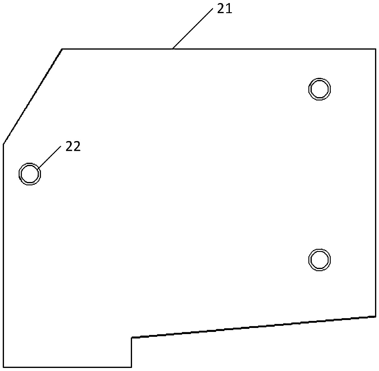
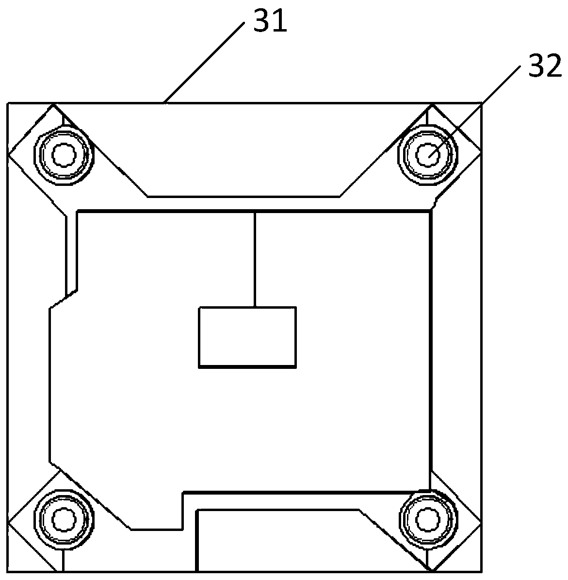
[0053] The core of the invention is to provide a method for editing the design drawing of the CPU in the PCB board. see Figure 1 to Figure 4 , in the prior art, each CPU package usually consists of a pin package, a fixture package, a heat sink package, and a backplane package. Layout engineers have to communicate with the organization department many times every time they do the layout of the CPU, so as to ensure the complete alignment between the pin package diagram, the fixture package diagram, the heat sink package diagram, and the backplane package diagram. If the alignment is inaccurate, it will cause damage to the CPU during loading and unloading, thus putting the product quality at risk.

[0054] However, in the design drawing editing method of CPU in a PCB board provided by the present invention, the preset CPU package drawing called includes the pin package drawing, the outline of the fixing piece corresponding to the fixing piece and the positioning hole of the fix...


PUM


Abstract

The invention discloses a method for editing a design drawing of a CPU (Central Processing Unit) in a PCB (Printed Circuit Board). The called preset CPU packaging drawing comprises a pin packaging drawing, a fixing piece contour line and a fixing piece positioning hole corresponding to a fixing piece, a cooling fin contour line and a cooling fin positioning hole corresponding to a cooling fin, anda backboard contour line corresponding to a backboard. That is to say, the preset CPU packaging diagram is essentially formed by adding and positioning the contour line and the positioning hole of the corresponding fixing piece in advance on the basis of the pin packaging diagram. According to the utility model, the radiating fins are arranged on the back plate, and corresponding to the contour lines and the positioning holes of the radiating fins and the contour line of the back plate, so that the original CPU packaging diagram consisting of four parts is integrated into the same packaging diagram, the alignment process during the design of the CPU packaging diagram is omitted, and the accurate alignment of each part in the CPU packaging diagram can be ensured at the same time. The invention further provides a design drawing editing device, design drawing editing equipment and a computer readable storage medium which have the same beneficial effects.

Description

technical field [0001] The present invention relates to the field of PCB technology, in particular to a method for editing a design drawing of a CPU in a PCB board, a device for editing a design drawing of a CPU in a PCB board, a device for editing a design drawing of a CPU in a PCB board, and a computer readable storage media. Background technique [0002] With the continuous advancement of science and technology in recent years, the structure and manufacturing process of PCB (printed circuit board) have achieved great development. [0003] At this stage, each control board will use a CPU (Central Processing Unit, central processing unit), and in the design drawing (Layout), a CPU package diagram usually consists of a pin package diagram, a fixture (ILM) package diagram, The package diagram of the heat sink (cooler) and the package diagram of the backplate (backplate). Among them, the pin package diagram corresponds to the pins of the CPU on the surface of the PCB board; ...

Claims


Application Information

Patent Timeline
IPC IPC(8): G06F17/50
Inventor 郭丹萍
Owner ZHENGZHOU YUNHAI INFORMATION TECH CO LTD
Learn More