
Semiconductor device buffer layer manufacturing method

A manufacturing method and buffer layer technology, applied in semiconductor/solid-state device manufacturing, semiconductor devices, electrical components, etc., can solve problems such as adverse effects on device switching characteristics, increased device manufacturing costs, and expensive high-energy ion implanters. Achieve the effect of optimizing carrier concentration distribution and increasing depth

Pending Publication Date: 2019-05-03
成都森未科技有限公司
View PDF11 Cites 1 Cited by
  • Summary
  • Abstract
  • Description
  • Claims
  • Application Information

AI Technical Summary

Problems solved by technology

However, the above-mentioned technology has two disadvantages: 1. Limited by the atomic mass or the diffusion ability of ions in the semiconductor, for the above-mentioned commonly used doping elements, it is necessary to form a deep n-type buffer layer and optimize the current carrying capacity with a large space Sub-concentration distribution, by requiring a high-energy ion implanter above 500KeV, and the price of a high-energy ion implanter is very expensive, which will greatly increase the manufacturing cost of the device in the mass production of the device
2. If you choose low-cost low-energy ion implantation, then in the case of only phosphorus implantation or proton implantation, the carrier concentration distribution often drops too fast at the interface between the n-type buffer layer and the n-type drift region, forming a very small Steep concentration distribution, which will adversely affect the switching characteristics of the device and other performance

Method used


Image

  • Semiconductor device buffer layer manufacturing method
  • Semiconductor device buffer layer manufacturing method
  • Semiconductor device buffer layer manufacturing method

Examples


Embodiment 1

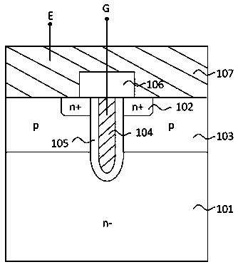
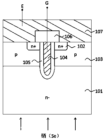
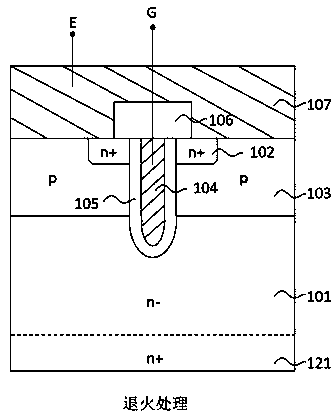
[0036] A method for manufacturing a semiconductor device buffer layer, forming an n-type buffer layer comprising a first n-type buffer layer and a second n-type buffer layer on a semiconductor substrate, or on the back of a semiconductor substrate having a p-type collector region formed on the back of the semiconductor substrate. A buffer layer, the first n-type buffer layer is formed by implanting selenium on the back of the semiconductor substrate and annealing after the implantation, and the second n-type buffer layer is formed by implanting protons on the back of the semiconductor substrate and annealing after the implantation , counting from the back surface of the semiconductor substrate, the depth of the first n-type buffer layer is deeper than the depth of the second n-type buffer layer, and the peak concentration of the first n-type buffer layer is lower than that of the second n-type buffer layer. The peak concentration of the n-type buffer layer is shallow. In the p...

Embodiment 2

[0038] A semiconductor device buffer layer manufacturing method, forming an n-type buffer layer including a first n-type buffer layer and a second n-type buffer layer on a semiconductor substrate, or on the back of a semiconductor substrate having a p-type collector region formed on the back of the semiconductor substrate , the first n-type buffer layer is formed by implanting selenium on the back of the semiconductor substrate and annealing after implantation, and the second n-type buffer layer is formed by implanting protons or phosphorus or implanting protons and phosphorus on the back of the semiconductor substrate The combination of implantation, annealing treatment is performed after implantation, counting from the back surface of the semiconductor substrate, the depth of the first n-type buffer layer is deeper than the depth of the second n-type buffer layer, and the first n-type buffer layer layer has a shallower peak concentration than the second n-type buffer layer. ...

Embodiment 3

[0050] A semiconductor device buffer layer manufacturing method, forming an n-type buffer layer including a first n-type buffer layer and a second n-type buffer layer on a semiconductor substrate, or on the back of a semiconductor substrate having a p-type collector region formed on the back of the semiconductor substrate , the first n-type buffer layer is formed by implanting selenium on the back of the semiconductor substrate and annealing after implantation, and the second n-type buffer layer is formed by implanting protons or phosphorus or implanting protons and phosphorus on the back of the semiconductor substrate The combination of implantation, annealing treatment is performed after implantation, counting from the back surface of the semiconductor substrate, the depth of the first n-type buffer layer is deeper than the depth of the second n-type buffer layer, and the first n-type buffer layer layer has a shallower peak concentration than the second n-type buffer layer. ...


PUM


Abstract

The present invention relates to the field of semiconductor device manufacture and in particular to a semiconductor device buffer layer manufacturing method. The semiconductor device comprises a semiconductor substrate, a first n-type buffer layer and a second n-type buffer layer. The first n-type buffer layer is formed by performing selenium implantation on the back surface of the semiconductor substrate and an annealing treatment after implantation. The second n-type buffer layer is formed by performing proton implantation or phosphorus implantation or a combination of proton implantation and phosphorus implantation on the back surface of the semiconductor substrate, and an annealing treatment after implantation. The method forms the first n-type buffer layer by implanting selenium elements capable of forming an n-type doping and having a high diffusion coefficient into the back surface of the semiconductor substrate, and forms a second n-type buffer layer by proton implantation witha small atomic mass or a common phosphorus implantation. Under a relative low-energy ion implantation condition, by the combination of the ion implantation of the above two elements and the annealingactivation, the depth of the n-type buffer layer is increased and the carrier concentration distribution of the n-type buffer layer and the device performance of the FS-IGBT are optimized.

Description

technical field [0001] The invention relates to the field of semiconductor device manufacturing, in particular to a method for manufacturing a semiconductor device buffer layer. Background technique [0002] In semiconductor devices such as diodes and insulated gate bipolar transistors (IGBTs), in order to reduce the thickness and loss of the device while ensuring the withstand voltage capability and switching performance of the device, it is necessary to dope the semiconductor substrate at a deeper position from the back of the device. , forming a buffer layer with a carrier concentration higher than that of the substrate. According to Poisson's equation, the electric field attenuation gradient is proportional to the charge concentration, so a buffer layer with a higher concentration can make the electric field rapidly decay and stop at this layer, preventing the depletion region from expanding to the back surface of the device and causing punchthrough, so the buffer layer ...

Claims


Application Information

Patent Timeline
IPC IPC(8): H01L21/331H01L29/06
Inventor 王思亮胡强蒋兴莉
Owner 成都森未科技有限公司
Learn More