High-precision, high-reliability multi-layer low-resistance thermal chip and method for making the same
A production method and high-precision technology, applied in the direction of resistance manufacturing, non-adjustable metal resistors, resistors, etc., can solve the problems of inability to miniaturize the production of microcircuits, decrease in product measurement sensitivity, and slow response speed, etc., to achieve effective Conducive to miniaturization, fast response, and small size
- Summary
- Abstract
- Description
- Claims
- Application Information
AI Technical Summary
Problems solved by technology
Method used
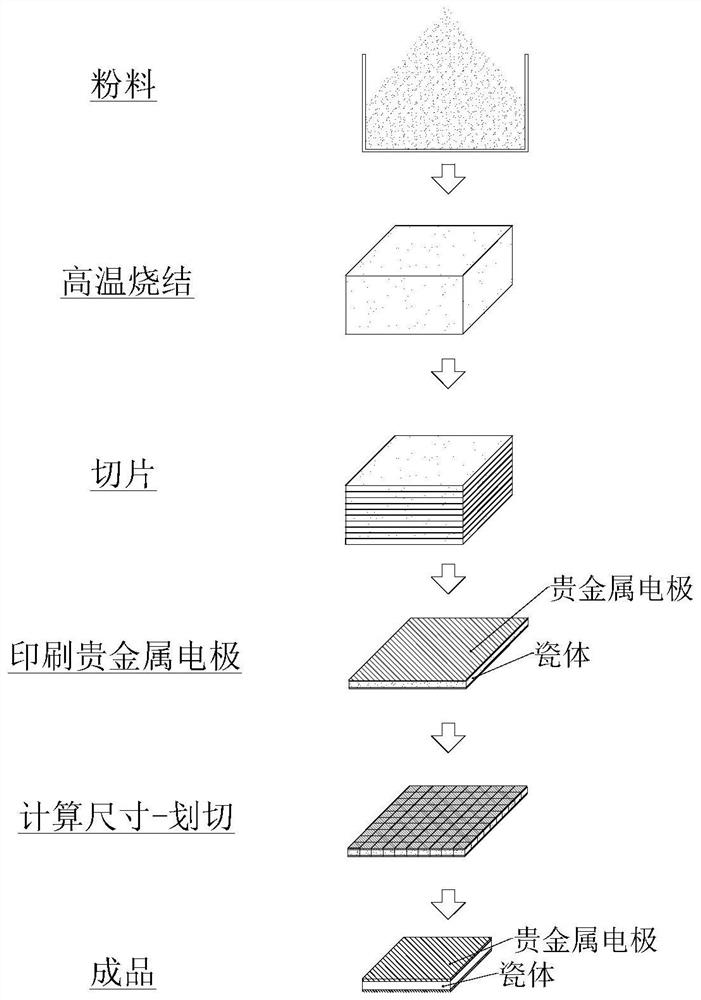
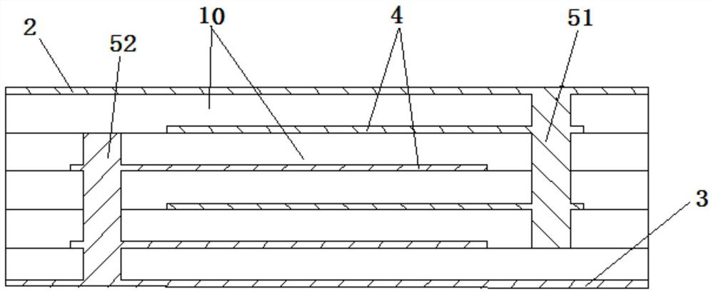
Image

Examples
Embodiment Construction
[0042] In the description of the present invention, it should be noted that for orientation words, such as the term "center", "horizontal (X)", "longitudinal (Y)", "vertical (Z)", "length", "width ", "Thickness", "Top", "Down", "Front", "Back", "Left", "Right", "Vertical", "Horizontal", "Top", "Bottom", "Inner" , "Outside", "Clockwise", "Counterclockwise", etc. indicating orientation and positional relationship are based on the orientation or positional relationship shown in the drawings, and are only for the convenience of describing the present invention and simplifying the description, rather than indicating or implying The devices or elements must have a specific orientation, be constructed and operated in a specific orientation, and should not be construed as limiting the specific protection scope of the present invention.
[0043] In addition, terms such as "first" and "second" are used for descriptive purposes only, and cannot be understood as indicating or implying rel...
PUM
| Property | Measurement | Unit |
|---|---|---|
| thickness | aaaaa | aaaaa |
| electrical resistivity | aaaaa | aaaaa |
| thickness | aaaaa | aaaaa |
Abstract
Description
Claims
Application Information
 - R&D
- Intellectual Property
- Life Sciences
- Materials
- Tech Scout
- Unparalleled Data Quality
- Higher Quality Content
- 60% Fewer Hallucinations
Browse by: Latest US Patents, China's latest patents, Technical Efficacy Thesaurus, Application Domain, Technology Topic, Popular Technical Reports.
© 2025 PatSnap. All rights reserved.Legal|Privacy policy|Modern Slavery Act Transparency Statement|Sitemap|About US| Contact US: help@patsnap.com