Carrier structure

A carrier board and substrate technology, which is applied in directions including printed inductors and printed electrical components, etc., can solve the problems of inability to meet the thinning and the overall thickness becoming thicker.

Active Publication Date: 2020-11-24
UNIMICRON TECH CORP
View PDF9 Cites 0 Cited by
  • Summary
  • Abstract
  • Description
  • Claims
  • Application Information

AI Technical Summary

Problems solved by technology

In this way, the overall thickness of the circuit carrier board will become thicker, which cannot meet the requirements of thinning

Method used


Image

  • Carrier structure
  • Carrier structure
  • Carrier structure

Examples


Embodiment Construction

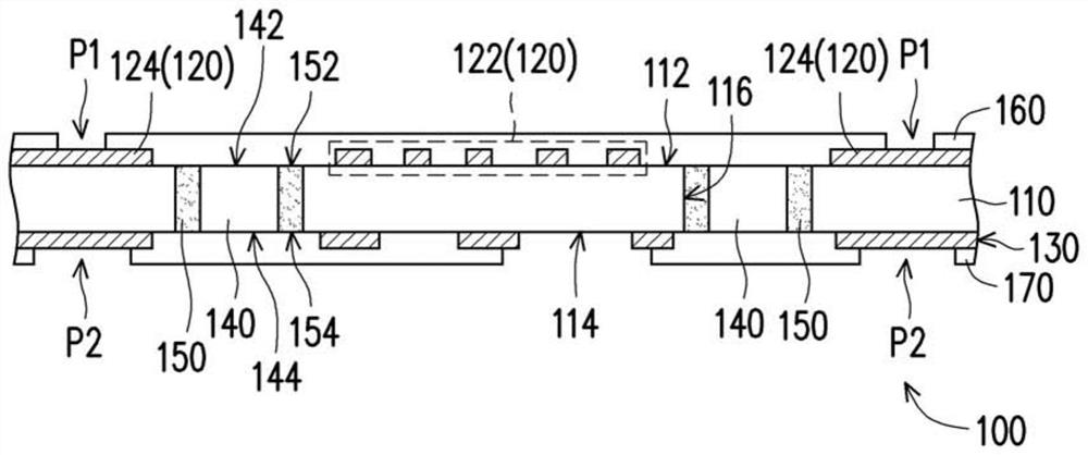
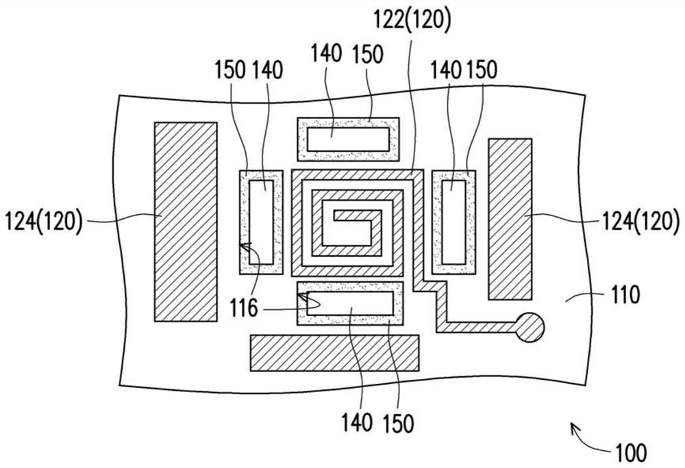
[0039] Figure 1A A schematic cross-sectional view of a carrier structure according to an embodiment of the present invention is shown. Figure 1B shown as Figure 1A The partial top view schematic diagram of the substrate structure. Figure 2A to Figure 2D shown as Figure 1A A schematic cross-sectional view of a manufacturing method of a carrier structure. For the sake of illustration, Figure 1B Some components, such as the first solder resist layer, are omitted in .

[0040] Please also refer to Figure 1A and Figure 1B , the carrier structure 100 of this embodiment includes a substrate 110 , a first patterned circuit layer 120 and at least one magnetic element 140 (four are schematically shown in 1B). The substrate 110 has a first surface 112 and at least one opening 116 (four are schematically shown in IB) extending through the substrate. The first patterned circuit layer 120 is disposed on the first surface 112 of the substrate 110 and includes a loop circuit 122 f...


PUM


Abstract

The present invention provides a carrier structure. The carrier structure comprises a substrate, a first patterned wiring layer and at least one magnetic component. The substrate has a first surface and at least one opening penetrating the substrate. The first patterned wiring layer is disposed on the first surface of the substrate and includes an annular line for generating an electromagnetic field. The at least one magnetic component is disposed in the opening of the substrate, wherein the at least one magnetic component is coupled to the annular line and acts in response to the magnetic force effect of the electromagnetic field.

Description

technical field [0001] The invention relates to a carrier structure, in particular to a carrier structure embedded with magnetic elements. Background technique [0002] Generally speaking, the circuit carrier needs to pass through the design of the ring circuit to generate an electromagnetic field. In order to increase the magnetic effect of the electromagnetic field, it is necessary to add magnetic elements above and / or below the ring circuit in a layer-building manner. As a result, the overall thickness of the circuit carrier will become thicker, which cannot meet the requirement of thinning. Contents of the invention [0003] The invention provides a carrier structure with inductive effect and thinner thickness. [0004] The carrier structure of the present invention includes a substrate, a first patterned circuit layer and at least one magnetic element. The substrate has a first surface and at least one opening through the substrate. The first patterned circuit lay...

Claims


Application Information

Patent Timeline
Patent Type & Authority Patents(China)
IPC IPC(8): H05K1/16
CPCH05K1/165
Inventor 陈昌甫陈君豪吴冠曦潘彼得
Owner UNIMICRON TECH CORP
Why Eureka
Try Eureka