A method of riveting pcb circuit board using rivets

A PCB circuit board, rivet technology, applied in the direction of rivets, applications, household appliances, etc., to achieve the effect of solving scrap, strong positioning support, and reducing manpower

Active Publication Date: 2020-11-17
昆山敏欣电子有限公司
View PDF3 Cites 0 Cited by
  • Summary
  • Abstract
  • Description
  • Claims
  • Application Information

AI Technical Summary

Problems solved by technology

[0003] The technical problem to be solved by the present invention is to provide a new rivet for PCB circuit board riveting and its manufacturing process in view of the above-mentioned deficiencies in the prior art. The inner short scrapping caused by rivet chipping and the scrapping caused by layer deviation caused by rivet deformation can reduce manpower and material costs

Method used


Image

  • A method of riveting pcb circuit board using rivets

Examples


Embodiment Construction

[0014] The specific embodiment of the present invention is further described below in conjunction with accompanying drawing:

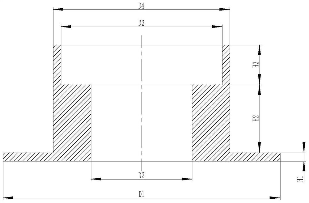
[0015] A method for pressing a PCB circuit board with rivets, the rivet is an inverted "T" structure, the center of the rivet is provided with a counterbore, and the diameter D1 of the flange at the bottom of the rivet is 2.0-8.0 mm, The height H1 of the flange plate at the bottom of the rivet is 0.1-1.0 mm, the small diameter D2 of the central counterbore hole of the rivet is 0.5-4.0 mm, the major diameter D3 of the central counterbore hole of the rivet is 1.0-4.5 mm, and the The outer diameter D4 of the upper end of the rivet is 1.5-5.0mm, the distance H2 between the large-diameter bottom surface of the rivet center counterbore and the top surface of the rivet bottom flange is 0.1-10.0mm, and the rivet top surface and the rivet center sink The distance H3 between the large-diameter bottom surfaces of the holes is 0.3-6.0 mm.

[0016] In an embodimen...


PUM

PropertyMeasurementUnit
diameteraaaaaaaaaa
heightaaaaaaaaaa
diameteraaaaaaaaaa

Abstract

The invention discloses a brand new rivet suitable for PCB circuit board riveting and a manufacturing process thereof. The rivet is characterized in that the rivet is of an inverted-T structure, a sinking hole is formed in the center of the rivet, the diameter D1 of a bottom flange disc of the rivet ranges from 2.0 to 8.0 mm, the height H1 of the bottom flange disc of the rivet ranges from 0.1 to1.0 mm, the small diameter D2 of the sinking hole in the center of the rivet ranges from 0.5 to 4.0 mm, the large diameter D3 of the sinking hole in the center of the rivet ranges from 1.0 to 4.5 mm,the outer diameter D4 of the upper end of the rivet ranges from 1.5 to 5.0 mm, the distance H2 between the large-diameter bottom face of the sinking hole in the center of the rivet and the top face ofthe bottom flange disc of the rivet ranges from 0.1 mm to 10.0 mm, and the distance H3 between the top face of the rivet and the large-diameter bottom face of the sinking hole in the center of the rivet ranges from 0.3 to 6.0 mm. The rivet has the advantages that scraps do not fall off, and layer deviation is avoided, the problem that in the riveting process, scrapping is caused by inner short scrapping caused by rivet scrap falling and layer deviating caused by rivet deforming can be solved, and manpower and material cost can be reduced.

Description

technical field [0001] The invention belongs to the technical field of rivets, and in particular relates to a method for riveting a PCB circuit board with a rivet. Background technique [0002] At present, when the existing rivets are used for riveting multi-layer circuit boards, on the one hand, they are prone to chipping, which leads to a short circuit in the circuit board due to chipping, which leads to the scrapping of the circuit board; scrapped. Therefore, the operating efficiency is greatly reduced, the production cost is increased, and the product quality is reduced. Contents of the invention [0003] The technical problem to be solved by the present invention is to provide a new rivet for PCB circuit board riveting and its manufacturing process in view of the above-mentioned deficiencies in the prior art. The inner short scrap caused by rivet chipping and the scrap caused by layer deviation caused by rivet deformation can reduce manpower and material costs. [...

Claims


Application Information

Patent Timeline
Patent Type & Authority Patents(China)
IPC IPC(8): B29C65/60F16B19/08F16B5/04B29L31/34
CPCB29C65/602B29L2031/3425F16B5/04F16B19/08
Inventor 庄召国张远武
Owner 昆山敏欣电子有限公司
Why Eureka
Try Eureka