Polarization-independent grating based on covered refractive index matching layer and its preparation method
A refractive index matching layer and refractive index technology, which is applied in the optical field, can solve the problem that the design of polarization-independent gratings is relatively difficult, and achieve the effect of simple and efficient preparation method and high preparation tolerance.
- Summary
- Abstract
- Description
- Claims
- Application Information
AI Technical Summary
Problems solved by technology
Method used
Image
Examples
Embodiment 1
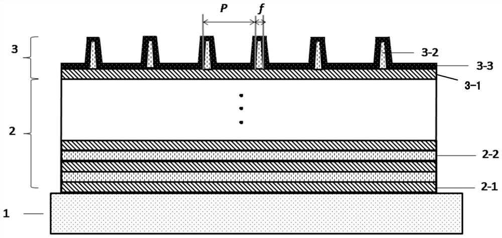
[0033] Such as figure 1 As shown, it is a polarization-independent reflective dielectric grating covered with a refractive index matching layer for a central wavelength of 1064nm. The diffraction efficiency of -1 order is higher than 98.5% in the bandwidth range of 1050-1080nm under the incident light of the state under the incident condition of Littrow angle.
[0034] The grating includes a fused silica substrate 1, on which a reflective film 2 and a grating functional layer 3 are sequentially plated; the grating functional layer 3 includes an oxide dielectric film connection layer 3-1, a single-layer oxide The object dielectric film grating layer 3-2 and the refractive index matching layer 3-3, and the single-layer oxide dielectric film grating layer 3-2 is etched into a grating groove structure.
[0035] The reflective film 2 is a multi-layer dielectric thin film with adjustable refractive index, and the number of periods is 14, which includes a high refractive index mater...
Embodiment 2
[0041] This embodiment is used to describe in detail the preparation method of the polarization-independent reflective dielectric grating covered with the refractive index matching layer in any of the foregoing embodiments.
[0042] Described preparation method comprises the steps:
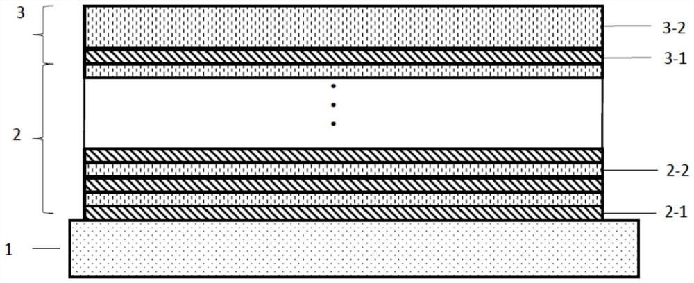
[0043] S1, on the fused silica substrate 1, the reflective film 2, the oxide dielectric film connection layer 3-1, and the single-layer oxide dielectric film grating layer 3-2 are sequentially plated, such as figure 2 shown;
[0044] The single-layer oxide dielectric film grating layer 3-2 is prepared by ion beam sputtering or electron beam evaporation, and its material is SiO 2 ;
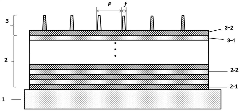
[0045] S2, on the single-layer oxide dielectric film grating layer 3-2, prepare a grating mask by holographic exposure or electron beam exposure, and perform grating groove etching by reactive ion etching, such as image 3 shown;
[0046] The groove structure of the grating is a rectangular groove or a trapezoidal...
PUM
| Property | Measurement | Unit |
|---|---|---|
| thickness | aaaaa | aaaaa |
| thickness | aaaaa | aaaaa |
| thickness | aaaaa | aaaaa |
Abstract
Description
Claims
Application Information
 - Generate Ideas
- Intellectual Property
- Life Sciences
- Materials
- Tech Scout
- Unparalleled Data Quality
- Higher Quality Content
- 60% Fewer Hallucinations
Browse by: Latest US Patents, China's latest patents, Technical Efficacy Thesaurus, Application Domain, Technology Topic, Popular Technical Reports.
© 2025 PatSnap. All rights reserved.Legal|Privacy policy|Modern Slavery Act Transparency Statement|Sitemap|About US| Contact US: help@patsnap.com


