Three-dimensional packaging structure and method

A packaging structure, three-dimensional technology, applied in the direction of microstructure technology, microstructure devices, manufacturing microstructure devices, etc., can solve the problem of inability to realize three-dimensional packaging, face-to-face sensing or detection of upper and lower chips, lack of internal cavity and three-dimensional Three-dimensional requirements and other issues to achieve the effect of preventing damage to the chip structure

Pending Publication Date: 2019-03-12
山东盛芯电子科技有限公司
View PDF0 Cites 1 Cited by
  • Summary
  • Abstract
  • Description
  • Claims
  • Application Information

AI Technical Summary

Problems solved by technology

[0005] However, this kind of stacked packaging structure of multiple chips can only be based on the bottom substrate layer by layer, and cannot realize three-dimensional packaging. The need for direct contact of colloids, it can be seen that the above-mentioned conventional stacked packaging structure technology does not have the requirements for internal cavity and three-dimensional

Method used


Image

  • Three-dimensional packaging structure and method
  • Three-dimensional packaging structure and method

Examples


Embodiment 1

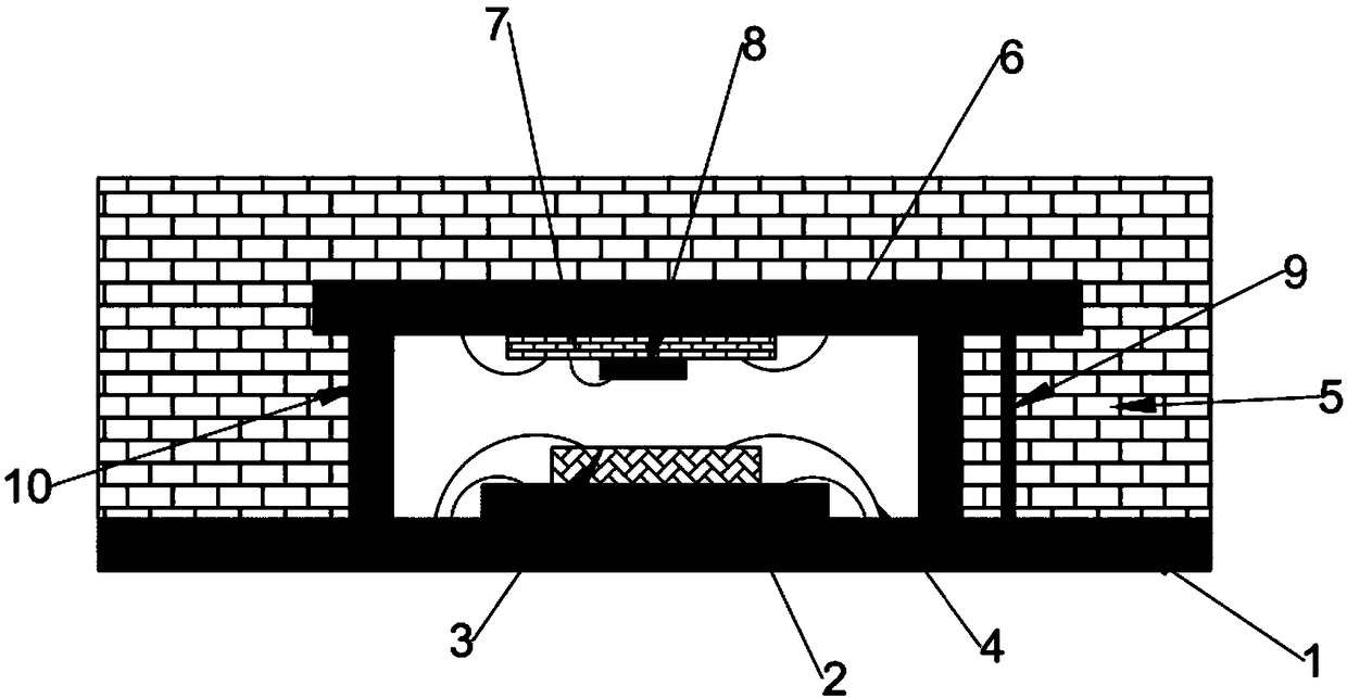
[0031] Example 1, such as figure 2 As shown, the present application provides a three-dimensional packaging structure, including an upper board 6 and a lower board 1, the upper board 6 and the lower board 1 are fixedly connected through a cavity support structure 10, and the cavity support structure 10 An installation space is formed between the upper board 6 and the lower board 1;

[0032] Specifically, the size and shape of the cavity support structure 10 can be designed and processed according to the actual product information, and can be regular shapes such as rectangles and circles, or irregular shapes, and the height is determined by the chip devices mounted inside and the distance between devices Decide. The cavity support structure 10 can be glued to the upper board 6 and the lower board 1 , or can be assembled by soldering. According to different types of chips integrated in the cavity, the cavity supporting structure 10 may be made of different materials such as m...

Embodiment 2

[0041] Example 2, such as figure 2 As shown, the present application provides a packaging method for a three-dimensional packaging structure, comprising the following steps:

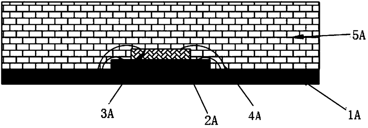
[0042] Step 1, mount the first chip 2 on the upper surface of the download board 1, mount the second chip 3 (MEMS chip) in micro-assembly, and connect the first chip 2, the second chip 3 and the download board 1 by wire bonding Electrical interconnection to complete the module structure of the download board 1;

[0043] Step 2, mount the third chip 7 and the fourth chip 8 (optical detection sensor chip) on the lower surface of the upper board 6, and electrically interconnect the third chip 7, the fourth chip 8 and the upper board 6 by wire bonding. Connect, complete the module structure of the upload board 6;

[0044] Step 3, assembling and installing the cavity supporting structure 10 on the assembled loading board 1 by gluing or metal welding;

[0045] Step 4, aligning and mounting the upper board ...


PUM


Abstract

The invention belongs to the field of chip packaging technology, in particular to a three-dimensional packaging structure and method. The three-dimensional packaging structure comprises an upper carrying plate and a lower carrying plate, wherein the upper carrying plate and the lower carrying plate are fixedly connected with each other through a cavity support structure; a mounting space is formedbetween the cavity support structure and the upper carrying plate and the lower carrying plate; chips are arranged on the lower surface of the upper carrying plate and the upper surface of the lowercarrying plate; the chips are arranged in the mounting space; the chips are electrically connected with the upper carrying plate or the lower carrying plate through a metal wire respectively; the electrical communication between the upper carrying plate and the lower carrying plate is realized by a conductor. Through adoption of the three-dimensional packaging structure and method, face-to-face induction and detection requirements of the chips are realized through the internal cavity structure under the condition of increasing the chip density of a packaging body, thereby realizing three-dimensional packaging.

Description

technical field [0001] The invention belongs to the technical field of chip packaging, and in particular relates to a three-dimensional packaging structure and method. Background technique [0002] With the vigorous development of the electronics industry, electronic products are also designed towards the trend of short, small, light, and thin. System-in-package SiP has become a common technology for improving chip packaging density and realizing system integration in packages. For example, in the previous multi-chip stacked packaging structure, multiple chips were stacked and sealed in a packaging material to achieve the miniaturization of chip packaging and the requirements of system integration in the package. Multiple chips will be integrated in one packaging structure. , in order to achieve more than twice the capacity or the functional requirements of systematic design. [0003] Generally speaking, among the known multi-chip packaging technologies, it is common to fi...

Claims


Application Information

Patent Timeline
IPC IPC(8): H01L25/16H01L23/31H01L21/98B81B7/00B81C1/00
CPCH01L25/162H01L25/165H01L25/50H01L23/3107B81B7/0074B81C1/00261H01L2224/48091H01L2924/00014
Inventor 刘昭麟邢广军
Owner 山东盛芯电子科技有限公司
Why Eureka
Try Eureka