
Rigid-flexible printed circuit board and manufacturing method thereof

A technology of soft-rigid combination board and production method, which is applied in the direction of multi-layer circuit manufacturing, printed circuit manufacturing, conductive pattern layout details, etc., can solve the problems of residual glue risk of protective tape, difficulty in laminating, difficulty in opening cover, etc., and achieve saving Adhesive barrier film bonding process, improving the efficiency of opening the cover, and increasing the effect of wiring density

Inactive Publication Date: 2019-03-05
AVARY HLDG (SHENZHEN) CO LTD +1
View PDF4 Cites 7 Cited by
  • Summary
  • Abstract
  • Description
  • Claims
  • Application Information

AI Technical Summary

Problems solved by technology

The disadvantage of using the above method is that there is a risk of residual glue when using protective tape such as PI / PET; the thickness of the protective tape is thicker, generally above 50um, which will cause height difference in lamination and cause uneven thickness of the interlayer; The protective adhesive (12um) is expensive, difficult to fit, and the protective tape is easily damaged; the protective tape has adhesive force with the inner FPC, and it is difficult to open the cover; UV fixed depth cutting is required, the precision control is strict, and the cost rises

Method used


Image

  • Rigid-flexible printed circuit board and manufacturing method thereof
  • Rigid-flexible printed circuit board and manufacturing method thereof
  • Rigid-flexible printed circuit board and manufacturing method thereof

Examples


no. 1 example

[0054] see Figure 1-7, the first embodiment of the present invention provides a method for manufacturing a rigid-flex board 100, which includes the steps of:

[0055] For a first step, see figure 1 , providing a flexible circuit board 10, the flexible circuit board may be a single-sided circuit board, a double-sided circuit board or a multi-layer board. In this embodiment, a double-sided circuit board is taken as an example for description.

[0056] The flexible circuit board 10 includes a flexible board substrate 13 , a first conductive circuit layer 11 , a second conductive circuit layer 12 and a first conductive hole 14 located on opposite surfaces of the flexible board substrate 13 . The second conductive circuit layer 12 is electrically connected to the first conductive circuit layer 11 through the first conductive hole 14 .

[0057] The number of the first conductive hole 14 may be multiple, or only one. The first conductive hole 14 can be a conductive via hole that...

no. 2 example

[0068] see Figure 8-12 The first step to the third step of the manufacturing method of the rigid-flex board provided by the second embodiment are the same as the first step to the third step of the manufacturing method of the rigid-flex board provided by the first embodiment. The reason is that in this embodiment, the step of opening the window has been completed before the surface build-up of the first double-sided adhesive film and the second double-sided adhesive film, that is, there is no need to etch away the first double-sided adhesive film after pressing. The first copper foil 41 and the second copper foil 42 at the positions of the opening 301a and the second opening 301b. The fourth step in this embodiment is specifically as follows:

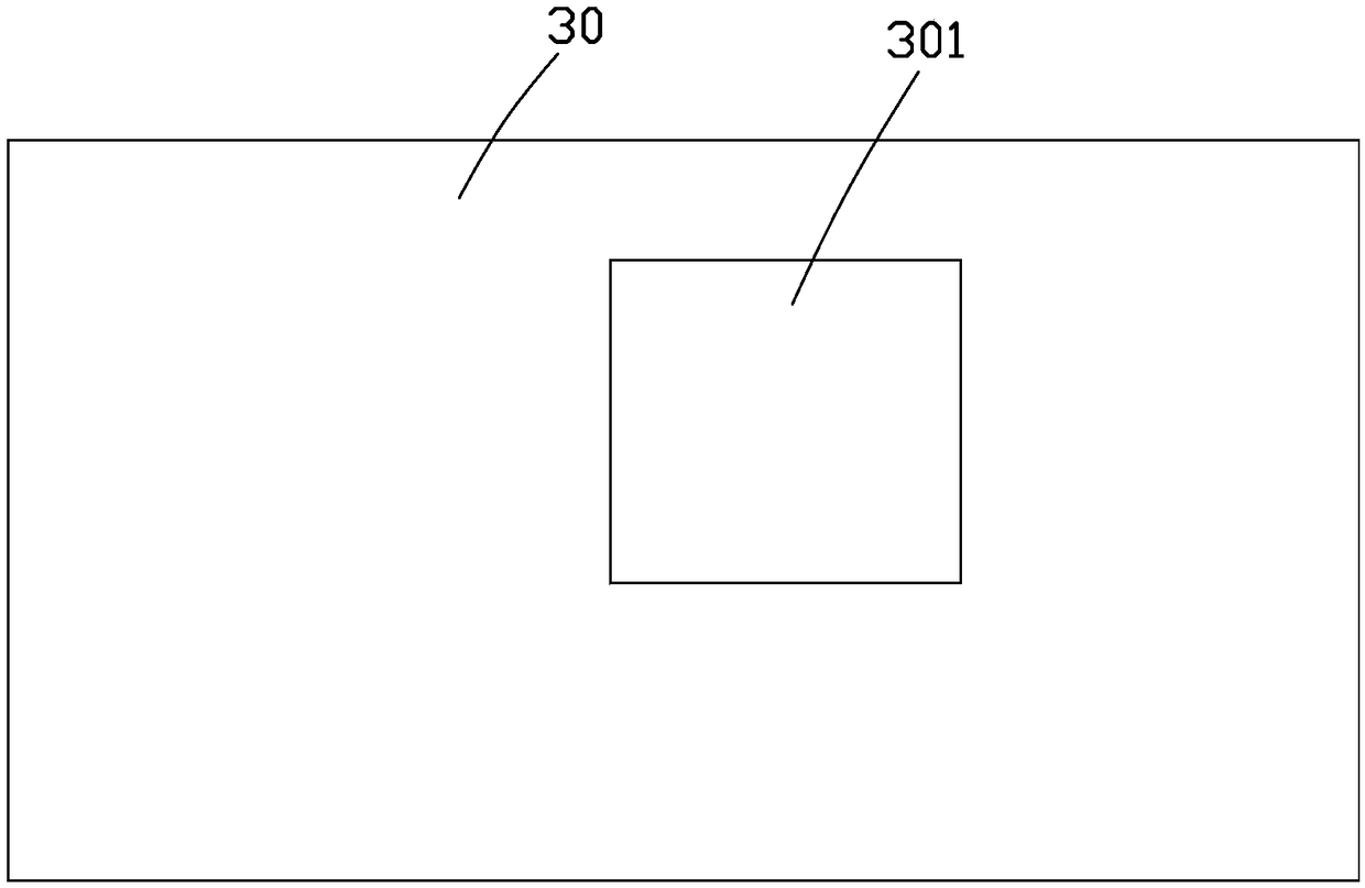
[0069] Step four, see Figure 8 , providing two copper-clad substrates 60, the copper-clad substrate 60 includes a dielectric layer 30 and a copper foil 40 formed on at least one surface of the dielectric layer 30; please refer to ...

no. 3 example

[0072] see again Figure 7 , the third embodiment of the present invention provides a rigid-flex board 100, which includes: a flexible circuit board 10, a first double-sided adhesive film 20a located on one surface of the flexible circuit board 10, a first double-sided adhesive film 20a located on the first double-sided The first dielectric layer 31 on the surface of the adhesive film 20a, the first outer conductive circuit layer 410 located on the surface of the first dielectric layer 31; the second double-sided adhesive film 20b located on the other surface of the flexible circuit board 10, located on the second The second dielectric layer 32 on the surface of the double-sided adhesive film 20b, the second outer conductive circuit layer 420 on the second dielectric layer 32 surface, and the first outer conductive circuit layer 410 and the second outer conductive circuit layer respectively The solder resist layer 53 on the surface of 420.

[0073] The flexible circuit board ...


PUM


Abstract

The invention relates to a rigid-flexible printed circuit board. The rigid-flexible printed circuit board comprises a flexible printed circuit board, wherein the flexible printed circuit board comprises a flexible printed circuit board base material and a first conductive circuit layer formed on at least one surface of the flexible printed circuit board base material, a double-sided adhesive filmformed on the surface of the first conductive circuit layer, a dielectric layer formed on the double-sided adhesive film, an outer layer conductive circuit layer formed on the surface of the dielectric layer, and a conductive hole, wherein the double-sided adhesive film comprises an insulating layer, and a first bonding layer and a second bonding layer, wherein the first bonding layer and the second bonding layer are formed on the two opposite surfaces of the insulating layer; the first bonding layer is in contact with the first conductive circuit layer; the dielectric layer comprises a firstopening, wherein the first opening exposes a part of the second bonding layer to form a flexible printed circuit board region; the conductive hole penetrates through the outer layer conductive circuitlayer to the first conductive circuit layer; and the outer layer conductive circuit layer is electrically connected with the first conductive circuit layer through the conductive hole.

Description

technical field [0001] The invention relates to circuit board manufacturing technology, in particular to a method for manufacturing a rigid-flex board and a rigid-flex board manufactured by the method. Background technique [0002] Rigid-Flexible Printed Circuit Board (Rigid-Flexible Printed Circuit Board, R-F PCB) refers to a printed circuit board that contains one or more rigid regions and one or more flexible regions. Circuit board) durability and soft board (Flexible Printed Circuit Board, FPCB, flexible circuit board), which has the characteristics of thinness, compactness and resistance to harsh application environments, especially suitable for portable electronic products, medical electronic products, military equipment and other precision electronics applications. [0003] At present, the main process of producing thin flexible and rigid boards is as follows: a. Punching / cutting a slit in the base material (PP) on the soft board; b. Sticking a layer of PI film with ...

Claims


Application Information

Patent Timeline
IPC IPC(8): H05K3/46H05K1/02
CPCH05K1/0298H05K3/4691H05K2203/12
Inventor 李彪杨文清黄美华钟浩文亢晓卫贾梦璐
Owner AVARY HLDG (SHENZHEN) CO LTD
Learn More