Reducing read disturb in memory device during signal switching transients

A memory cell, unselected technology, applied in the field of operation of memory devices

Active Publication Date: 2019-03-05
SANDISK TECH LLC
View PDF4 Cites 4 Cited by
  • Summary
  • Abstract
  • Description
  • Claims
  • Application Information

AI Technical Summary

Problems solved by technology

However, various challenges exist in operating such memory devices

Method used


Image

  • Reducing read disturb in memory device during signal switching transients
  • Reducing read disturb in memory device during signal switching transients
  • Reducing read disturb in memory device during signal switching transients

Examples


Embodiment Construction

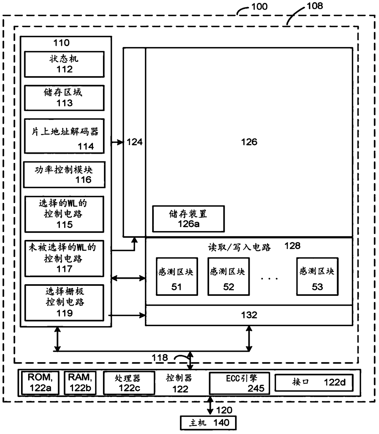
[0044] An apparatus and technique are described for reducing read disturb in a memory device.

[0045] In some memory devices, such as in NAND strings in blocks or sub-blocks, memory cells are connected to each other. Each NAND string consists of several memory cells connected in series between one or more select gate (SG) transistors on the drain side (referred to as SGD transistors) and one or more source-terminal SG transistors (referred to as SGS transistors), which One or more drain select gate (SG) transistors are on the drain terminal of the NAND string connected to the bit line, and the one or more source terminal SG transistors are on the source terminal of the NAND string connected to the source line. In addition, the memory cells may be arranged with a common control gate line (eg, a word line) serving as a control gate. A set of word lines extends from the source side of the block to the drain side of the block. The memory cells can be connected in other types of...


PUM


Abstract

A memory device and associated techniques for reducing read disturb of memory cells during a sensing process. Select gate transistors are transitioned to a conductive state one or more time during a sensing process, at the drain and / or source ends of the memory strings in an unselected sub-block. The transitioning can occur periodically, multiple times during the sensing process. When the select gate transistors are in a conductive state, accumulated holes in the channel can be removed. This help provide a faster decrease of the channel potential when the unselected word line voltages are ramped down at the end of the sensing process. The duration of a disturb-inducing channel gradient which is created next to the edge data memory cell is reduced so that read disturb of this cell is also reduced.

Description

technical field [0001] The present disclosure relates to the operation of memory devices. Background technique [0002] The use of semiconductor memory devices in various electronic devices has become more popular. For example, non-volatile semiconductor memory is used in cellular telephones, digital cameras, personal digital assistants, mobile computing devices, non-mobile computing devices, and other devices. [0003] Charge storage materials, such as floating gates or charge-trapping materials, can be used in such memory devices to store charges representative of data states. Charge-trapping materials may be arranged vertically in a three-dimensional (3D) stacked memory structure, or may be arranged horizontally in a two-dimensional (2D) memory structure. One example of a 3D memory structure is a cost-scalable (BiCS) architecture comprising alternating conductive and dielectric layers. [0004] The memory device includes memory cells, which may be arranged in strings, ...

Claims


Application Information

Patent Timeline
Patent Type & Authority Applications(China)
IPC IPC(8): G11C11/4094
CPCG11C11/4094G11C16/26G11C16/32G11C16/3418G11C16/3427G11C16/3459G11C16/0483G11C16/08G11C16/10G11C16/16
Inventor 陈宏燕赵伟卢景煌董颖达
Owner SANDISK TECH LLC
Why Eureka
Try Eureka