Fluorescent thin film structure for LED, preparation method thereof, and luminescent light source
A thin-film structure and fluorescence technology, applied in semiconductor devices, electrical components, circuits, etc., can solve the problems of phosphor deposition in dispensing process, avoid inconsistent dispensing uniformity, simple preparation method, and improve light color consistency Effect
- Summary
- Abstract
- Description
- Claims
- Application Information
AI Technical Summary
Problems solved by technology
Method used
Image
Examples
Embodiment 1
[0060] see figure 1 with figure 2 , the invention discloses a fluorescent film structure for LEDs, comprising a first transparent film 1; phosphor powder 2 coated on the upper surface of the first transparent film 1; and a second transparent film 3 attached to the phosphor powder 2 The upper surface of the first transparent film 1.
[0061]Since the density of the phosphor 2 is greater than that of the adhesive, under the action of gravity, the phosphor 2 precipitates and is not evenly distributed in the adhesive, resulting in a change in the concentration distribution of the phosphor adhesive. In addition, during the dispensing process, it is difficult to keep the concentration of phosphor 2 consistent from beginning to end. Phosphor 2 is mixed in the adhesive to maintain a certain particle size. During the dispensing process, the dispensing cylinder is placed vertically. A certain viscosity, but the density of phosphor 2 is greater than the density of the adhesive, phosph...
Embodiment 2
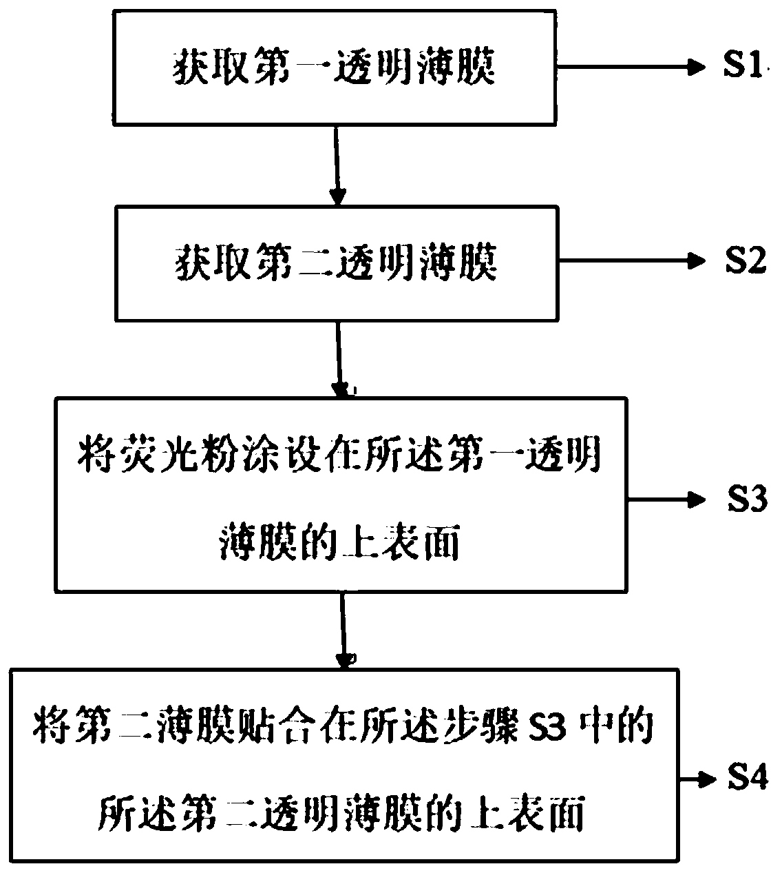
[0069] refer to image 3 , the present invention also discloses a method for preparing a fluorescent film structure for LEDs, comprising:
[0070] S1: Obtain the first transparent film 1;
[0071] S2: obtaining the second transparent film 3;
[0072] S3: coating the phosphor powder 2 on the upper surface of the first transparent film 1;
[0073] S4: attaching the second transparent film 3 to the upper surface of the first transparent film 1 in step S3 to form a fluorescent film structure for LED;
[0074] Step S1 and step S2 can be performed at the same time, and the order of step S2 and step S3 can be exchanged.
[0075] Specifically, step S1 includes:
[0076] S101: Weigh the first adhesive, and perform vacuum defoaming treatment on the first adhesive;
[0077] S102: Prepare a first transparent film-like adhesive on the substrate by using the first adhesive after vacuum degassing in step S101 by a spin coating method;
[0078] S103: Curing the first transparent film-li...
Embodiment 3
[0111] The invention also discloses an LED luminescent light source, which includes a fluorescent thin film structure for the LED. Encapsulating the fluorescent film structure into the LED light source can improve the light color consistency of the LED.
PUM
| Property | Measurement | Unit |
|---|---|---|
| thickness | aaaaa | aaaaa |
| thickness | aaaaa | aaaaa |
Abstract
Description
Claims
Application Information
 - Generate Ideas
- Intellectual Property
- Life Sciences
- Materials
- Tech Scout
- Unparalleled Data Quality
- Higher Quality Content
- 60% Fewer Hallucinations
Browse by: Latest US Patents, China's latest patents, Technical Efficacy Thesaurus, Application Domain, Technology Topic, Popular Technical Reports.
© 2025 PatSnap. All rights reserved.Legal|Privacy policy|Modern Slavery Act Transparency Statement|Sitemap|About US| Contact US: help@patsnap.com


