Tap coupling inductance type non-isolated DC boost converter and modulation method thereof
A coupled inductance, DC boost technology, applied in the direction of conversion equipment without intermediate conversion to AC, can solve the problems of weak boost capability of classic Boost topology and large voltage stress of switching tube.
- Summary
- Abstract
- Description
- Claims
- Application Information
AI Technical Summary
Problems solved by technology
Method used
Image
Examples
Embodiment 1
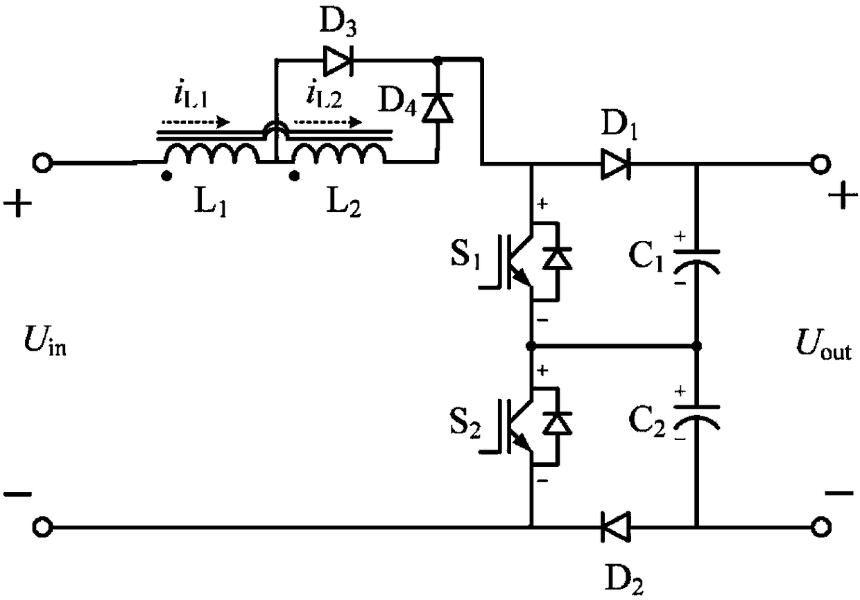
[0093] In the present invention, such as figure 1 The new circuit topology shown realizes non-isolated high ratio DC-DC boost conversion. The circuit topology is simple and clear, including: 1 coupled inductor (double winding) with a center tap; 2 fully controlled power electronic switching devices S 1 and S 2 (IGBT or MOSFET devices can be selected according to the voltage and power level in practical applications); 4 power diodes D 1 、D 2 、D 3 and D 4 ; 2 capacitors C 1 and C 2 ;
[0094] One end of the coupled inductor with a center tap is connected to the positive pole of the power supply input end, and the other end is connected to the anode of the fourth diode; the cathode of the fourth diode is respectively connected to the cathode of the third diode and the first diode. The anode of a diode is connected; the anode of the third diode is connected to the middle tap of the coupled inductor; the cathode of the first diode is connected to the positive pole of the po...
Embodiment 2
[0165] The simulation under MATLAB-SIMULINK is used as a verification case, such as figure 1 As shown, take the main circuit parameter C 1 =C 2 = 100μF, L 1s = L 2s =1.01mH L 1-2M =1mH, turns ratio N=1, where L 1s and L 2s Inductance L 1 and L 2 self-inductance, L 1-2M is the inductance L 1 with L 2 mutual inductance. In this example, under the condition of N=1, satisfy L 1s = L 2s ≈L 1-2M , which can be considered as an approximate ideal coupling situation.
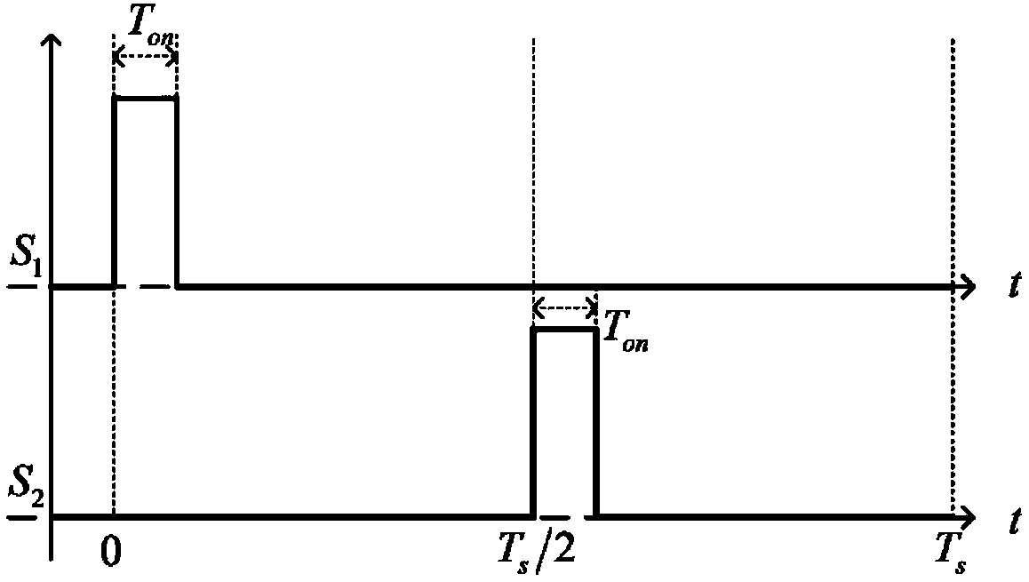
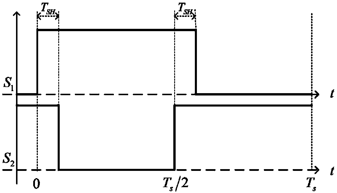
[0166]The input DC voltage is U in =800V, conduct open-loop simulation test in two modes of non-over-conduction modulation and over-conduction modulation, and take the conduction duty cycle G 1 =0.5, direct duty ratio G 2 =0.5, resistive load R L =100Ω, the obtained DC output voltage waveforms under transient state and steady state are respectively as attached Figure 5 (a / b / c) shown.
[0167] It can be seen that when the non-over-conduction modulation mode is adopted, the average value of the output ...
PUM
 Abstract
Description
Claims
Application Information
 - R&D
- Intellectual Property
- Life Sciences
- Materials
- Tech Scout
- Unparalleled Data Quality
- Higher Quality Content
- 60% Fewer Hallucinations
Browse by: Latest US Patents, China's latest patents, Technical Efficacy Thesaurus, Application Domain, Technology Topic, Popular Technical Reports.
© 2025 PatSnap. All rights reserved.Legal|Privacy policy|Modern Slavery Act Transparency Statement|Sitemap|About US| Contact US: help@patsnap.com


