Image sensor and manufacturing method thereof

An image sensor, pixel area technology, applied in semiconductor/solid-state device manufacturing, semiconductor devices, electro-solid devices, etc., can solve problems such as image quality degradation, easy saturation of white light pixels, and electron overflow

Active Publication Date: 2021-07-06
淮安西德工业设计有限公司
View PDF5 Cites 0 Cited by
  • Summary
  • Abstract
  • Description
  • Claims
  • Application Information

AI Technical Summary

Problems solved by technology

[0005] The technical problem to be solved by the technical solution of the present invention is to provide a new image sensor structure for the defect that the white light pixels in the existing image sensor are easily saturated, causing electrons to overflow into the adjacent photodiodes, thereby causing the image quality to decline Improving the imaging quality and imaging sensitivity of an image sensor under dark light and its manufacturing method

Method used


Image

  • Image sensor and manufacturing method thereof
  • Image sensor and manufacturing method thereof
  • Image sensor and manufacturing method thereof

Examples


Embodiment 2

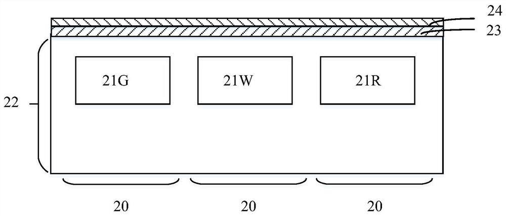
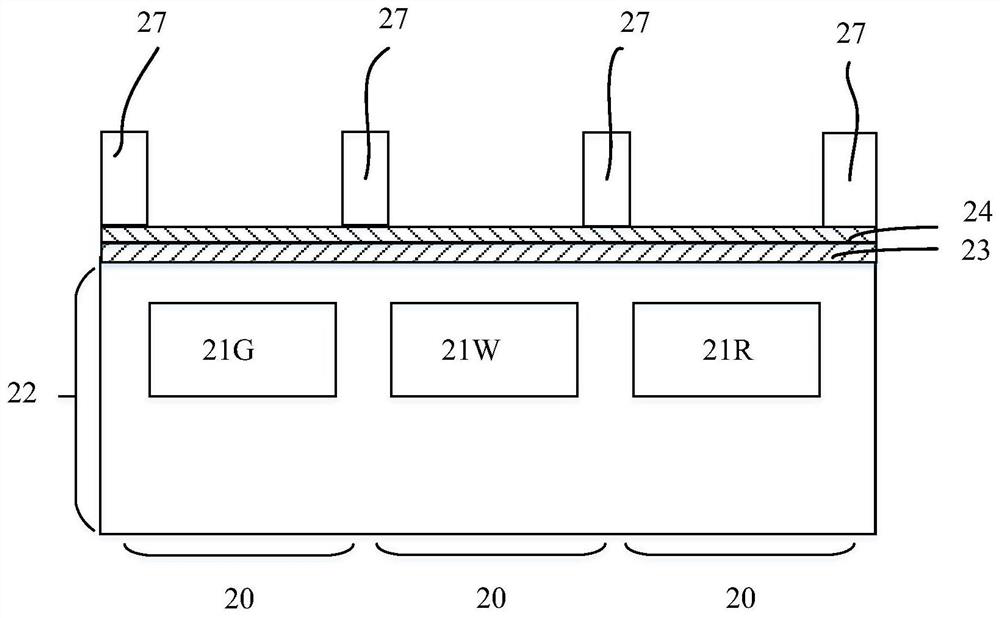
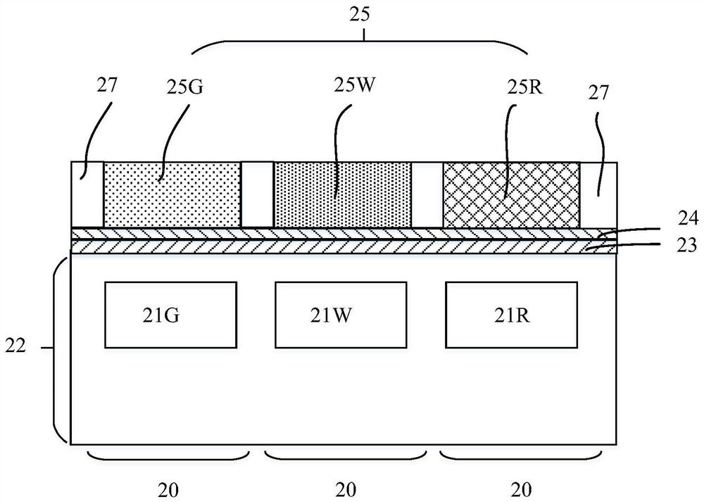
[0043] This embodiment provides an image sensor structure comprising: a semiconductor substrate 22 having a photodiode, the semiconductor substrate 22 comprising a different pixel region 20, wherein the photodiode corresponds to a different pixel region; located in the semiconductor substrate. The upper insulation structure; the light shielding film 27 located on the insulating structure, the light shielding film 27 cover the insulating structure and isolates the different pixel regions 20; the color filter layer 25 corresponding to different pixels is located in the insulating structure. The filter layer 25 includes a white color filter layer 25W; an organic photodiode 28 that blocks the white color filter layer and partially occluded in the white color filter; a microlens 26 located above the color filter layer 25.

[0044] Reference Figure 5 The semiconductor substrate 22 can be a silicon substrate, and may be germanium, silicon, silicon carbide, arsenide or gallium indium, or ...


PUM

PropertyMeasurementUnit
thicknessaaaaaaaaaa

Abstract

The technical solution of the present invention discloses an image sensor and a manufacturing method thereof. The image sensor includes a semiconductor substrate formed with a photodiode, and the semiconductor substrate includes different pixel areas, and the pixel area includes a white pixel area; An insulating structure on the insulating structure; a light-shielding film partially covering the insulating structure; a color filter layer corresponding to different pixels on the insulating structure, the color filter layer includes a white color filter layer, and the light-shielding film isolates the The color filter layer; an organic photodiode positioned above the white color filter layer and partially blocking the white color filter layer; a microlens positioned above the color filter layer. The image sensor not only improves the image quality of the image sensor, but also improves the sensitivity of the image sensor.

Description

Technical field [0001] The present invention relates to the field of manufacturing semiconductor devices, and more particularly to an image sensor and a method of making it. Background technique [0002] The image sensor is a device that converts an optical image into an electrical signal. With the development of computer and communication industries, the demand for high performance image sensors is growing, and these high-performance image sensors are widely used in digital camera, video camera, personal communication system (PCS), gaming machine, security camera, medical micro camera. Various areas such as. [0003] Image sensors are typically two types, chargeable devices (CCD) sensors, and CMOS image sensors (CMOSIMAGE SENSORS, CIS). Compared to the CCD image sensor, the CMOS image sensor has the advantages of high integration, small power consumption, low generation cost. [0004] In the conventional CMOS photosensitive element, the photosensitive diode is located behind the...

Claims


Application Information

Patent Timeline
Patent Type & Authority Patents(China)
IPC IPC(8): H01L27/30H01L51/48
CPCH10K39/32H10K71/00
Inventor 武海亮陈世杰黄晓橹
Owner 淮安西德工业设计有限公司
Why Eureka
Try Eureka