On-chip structure and communication method of broadcast based on micro-ring power divider and grouping

A technology of power divider and broadcast information, which is applied in the field of communication, and can solve the problems of low communication efficiency, cumbersomeness, and increased system energy consumption

Active Publication Date: 2019-01-22
XIDIAN UNIV
View PDF5 Cites 2 Cited by
  • Summary
  • Abstract
  • Description
  • Claims
  • Application Information

AI Technical Summary

Problems solved by technology

[0003] Zhan Su et al. from the Massachusetts Institute of Technology published an article "An on-chip partial drop wavelength selective broadcast network" in IEEE Lasers and Electro-Optics in 2014, disclosing a method of simultaneously coupling a light wave on a waveguide through 8 microrings to achieve The broadcast network, which can realize broadcast communication from one port to 8 ports at the same time, has high communication efficiency. In addition, the use of passive micro-ring resonators reduces the energy consumption of the on-chip control circuit, but the broadcast network is insufficient The reason is that only one node can broadcast to the remaining 8 nodes, and it is impossible to realize mutual broadcast between larger-scale nodes, and the scalability is limited
[0004] The application publication number is CN103442311A, and the patent application titled "Optical Network-on-Chip System Supporting Multicast Communication" discloses an optical network-on-chip system supporting multicast communication. The two-stage network composed of ring resonators realizes multicast communication between multiple nodes based on wavelength routing, and has certain scalability. Optical waveguide, and the radius relationship between multiple microrings needs to be finely controlled to achieve precise coupling of different wavelengths, which increases the difficulty of integrated design of on-chip optical structures. Active microrings require additional control circuits to change their coupling wavelengths, which increases the System control circuit energy consumption overhead; In terms of communication, using multiple wavelengths for multicast requires complex wavelength allocation strategies, and the on-chip optical wavelength resources are limited, which limits the scope of multicast communication, and the efficiency of multicast communication is low
This method takes a source node as the center and dynamically divides the 3D on-chip network into high and low partitions, and then the two partitions are further optimized and divided into multiple smaller sub-partitions according to a series of discriminant conditions. Broadcast information is routed in multiple sub-partitions. This communication method can realize independent multicasting in multiple regions after dynamic division. The operation is too complex and cumbersome, which increases the time overhead of multicast communication configuration, and the communication efficiency in the entire communication process between the source node and the destination node is still not high. In addition, the complex division operation requires additional circuit support, which increases the use of this method. broadcast system energy consumption

Method used


Image

  • On-chip structure and communication method of broadcast based on micro-ring power divider and grouping
  • On-chip structure and communication method of broadcast based on micro-ring power divider and grouping
  • On-chip structure and communication method of broadcast based on micro-ring power divider and grouping

Examples


Embodiment 1

[0082] refer to figure 1 , package, 16 super nodes 1, 4 global switching networks 2, 4 local switching networks 3 and 128 third optical waveguides 4, 16 super nodes 1 are divided into N groups, 4 in each group, in the nth group The mth super node 1 of the is denoted as S n,m ; The global switching network 2 includes four first microring power distributors 21; the local switching network 3 includes four second microring power distributors 31;

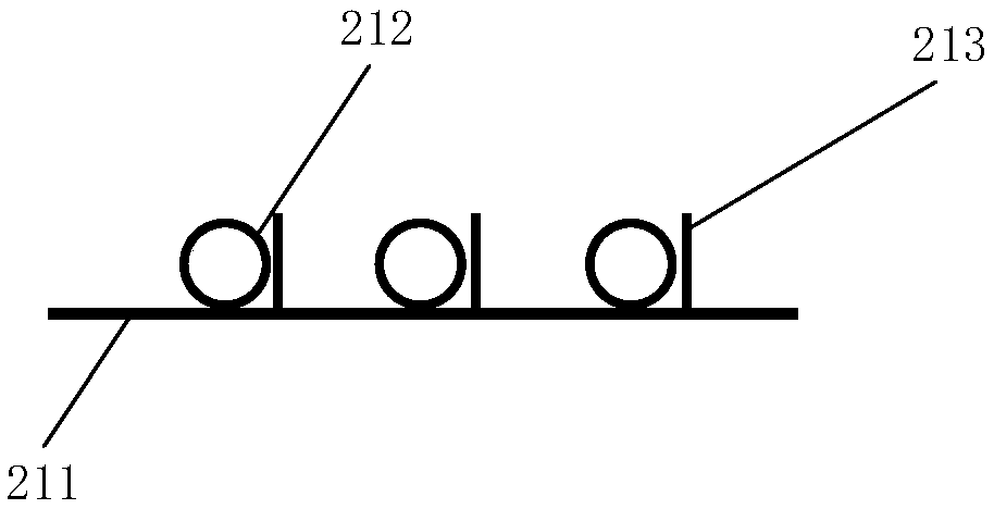
[0083] refer to figure 2 , the first microring power divider 21 includes a first main transmission optical waveguide 211, three first microring resonators 212 and three first auxiliary transmission optical waveguides 213; the first main transmission optical waveguide 211, It is used to couple the optical signal with a data bit width of 1 into the first microring resonator 212, and the first auxiliary transmission optical waveguide 213 is used to couple the first microring resonator 212 into the optical signal with a data bit width of ...

Embodiment 2

[0141] The structure of embodiment 2 is the same as that of embodiment 1, and the following parameters have been adjusted: the grouping of supernodes becomes 2 supernodes (M=2) in each group, and is divided into 4 groups (N=2) , the broadcast information is an electrical signal with a data bit width of 32 (B=32).


PUM


Abstract

The invention discloses an on-chip structure and a communication method of broadcast light based on a micro-ring power divider and an organization, for improving structural scalability and broadcast communication efficiency, reduce the difficulty of integrated design and the power consumption of control circuit, includes M * N super nodes, M globally switched networks, N local switching networks and M * N * (M+N) third optical waveguides, M >= 2, N >= 2, M * N super nodes are divided into N groups, each group M, the mth super node in the nth group is denoted by Sn, m, 1 <= n <= N, 1 <= m <= M,each super node includes M compute nodes, one crossover switch, two light modulators and M+N-2 optical demodulators, each global switching network includes N micro-ring power dividers, each local switching network includes M micro-ring power dividers, According to n, m, each super node connects a local switching network and a global switching network, and calculates the super node group number ofthe destination node and the number within the super node group to communicate with the local switching network, the global switching network or the local switching network and the global switching network.

Description

technical field [0001] The invention belongs to the technical field of communication, and relates to an on-chip optical interconnection structure and communication method, in particular to a broadcast optical on-chip structure and communication method based on a microring power divider and grouping, which can be used between computing nodes in a computing system broadcast communication. Background technique [0002] The on-chip optical interconnection structure realizes the communication between computing nodes in the computing system through the optical waveguide. In a computing system, besides unicast communication, there are also a large number of broadcast communications between computing nodes, so it is necessary to design an optical on-chip structure that supports broadcasting. Considering the broadcast traffic between a large number of computing nodes, the design of the broadcast optical on-chip structure and communication method mainly needs to solve the scalability...

Claims


Application Information

Patent Timeline
IPC IPC(8): H04Q11/00
CPCH04Q11/0005H04Q11/0062H04Q2011/0007H04Q2011/0047H04Q2011/0049H04Q2011/0058H04Q2011/0086
Inventor 顾华玺王康杨银堂王琨王玥
Owner XIDIAN UNIV
Why Eureka
Try Eureka