Optical sensor and electronic device
A technology of light sensor and light emitting part, which is applied in the field of light sensor to achieve the effect of high-precision distance measurement
- Summary
- Abstract
- Description
- Claims
- Application Information
AI Technical Summary
Problems solved by technology
Method used
Image

Examples
no. 1 approach 〕
[0032] refer to Figure 1 to Figure 7 A first embodiment of the present invention will be described.
[0033] (Schematic configuration of TOF sensor)
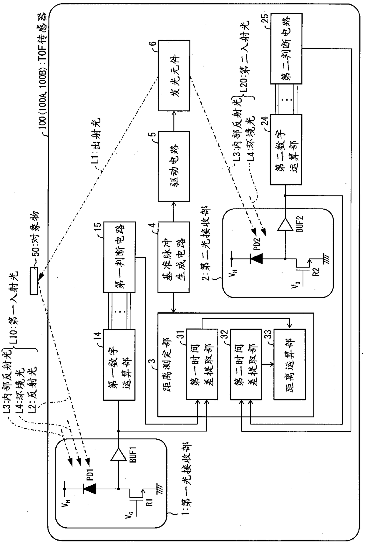
[0034] The TOF sensor 100 (optical sensor) measures the distance between the TOF sensor 100 and the object 50 by calculating the distance based on the time difference between the time when the light is emitted to the object and the time when the reflected light reflected by the object is received. The TOF sensor 100 is used in electronic devices such as smartphones and cameras, for example.
[0035] First, the schematic configuration of the TOF sensor 100 is summarized as follows.
[0036] The TOF sensor 100 includes: a light-emitting element 6 (light-emitting part), which emits light according to a reference pulse; a first light-receiving part 1, which outputs a first light-receiving pulse through light incidence; a first digital operation part 14 (a first calculation part) ), which is based on the number of first light-rec...
Deformed example 1
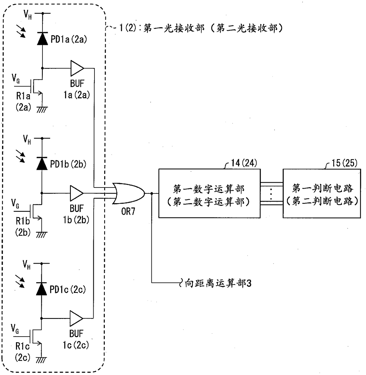
[0125] The following is based on Figure 7 , the first digital operation unit 141 as a modified example of the schematic configuration of the first digital operation unit 14 will be described. Figure 7 It is a block diagram showing a modified example of the configuration of the first digital operation unit 14 of the TOF sensor 100 . Furthermore, the circuit of the second digital operation unit 24 can also be configured in the same modified example as that of the first digital operation unit 14 .
[0126] The first digital operation unit 141 such as Figure 7 As shown, a lighting period counter 60 for counting the first output pulse number, a non-light-emitting period counter 61 for counting the second output pulse number, a multiplication circuit 62 for performing multiplication processing, and a subtraction circuit for performing subtraction processing may be respectively provided. 63. The light-emitting period counter 60 and the subtraction circuit 63, the non-light-emit...
no. 2 approach 〕
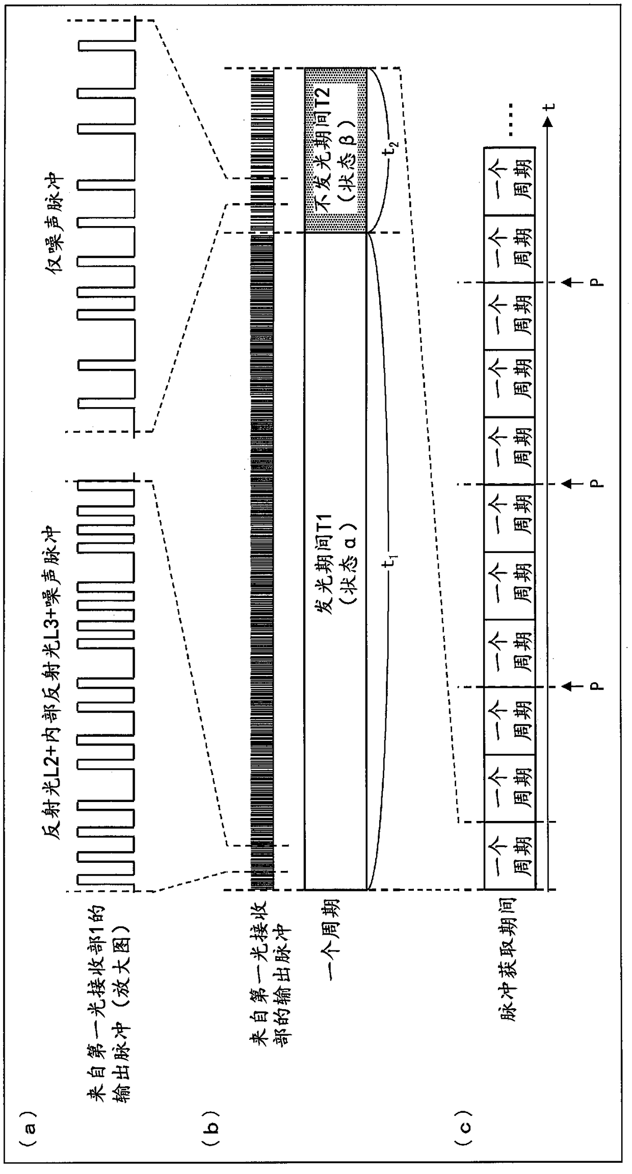
[0132] refer to figure 1 and Figure 8 , the second embodiment of the present invention will be described. Figure 8 It is a diagram for explaining the operation in the pulse acquisition period of the TOF sensor 100A according to the second embodiment of the present invention. The TOF sensor 100A differs from the TOF sensor 100 in that the light-emitting period T1 and the non-light-emitting period T2 are divided into one cycle, and other configurations are the same.
[0133] (Divide the light-emitting period and non-light-emitting period into one cycle)
[0134] In this embodiment, if Figure 8 As shown, the light-emitting period T1 and the non-light-emitting period T2 are divided into one cycle and implemented alternately. Specifically, the light-emitting period T1 is divided into a light-emitting period T11, a light-emitting period T12, and a light-emitting period T13 in one cycle, and the non-light-emitting period T2 is divided into a non-light-emitting period T21, a n...
PUM
 Abstract
Description
Claims
Application Information
 - Generate Ideas
- Intellectual Property
- Life Sciences
- Materials
- Tech Scout
- Unparalleled Data Quality
- Higher Quality Content
- 60% Fewer Hallucinations
Browse by: Latest US Patents, China's latest patents, Technical Efficacy Thesaurus, Application Domain, Technology Topic, Popular Technical Reports.
© 2025 PatSnap. All rights reserved.Legal|Privacy policy|Modern Slavery Act Transparency Statement|Sitemap|About US| Contact US: help@patsnap.com