Light emitting diode chip and preparation method thereof

A technology of light-emitting diodes and chips, applied in electrical components, circuits, semiconductor devices, etc., can solve the problem of high light absorption cost

Active Publication Date: 2019-01-11
ELEC TECH PHOTOELECTRIC TECH DALIAN
View PDF5 Cites 8 Cited by
  • Summary
  • Abstract
  • Description
  • Claims
  • Application Information

AI Technical Summary

Problems solved by technology

[0004] Based on the above, it is necessary to provide a light-emitting diode chip and its preparation method for the serious light absorption and relatively high cost problems in the preparation process of the light-emitting diode chip

Method used


Image

  • Light emitting diode chip and preparation method thereof
  • Light emitting diode chip and preparation method thereof
  • Light emitting diode chip and preparation method thereof

Examples


Embodiment Construction

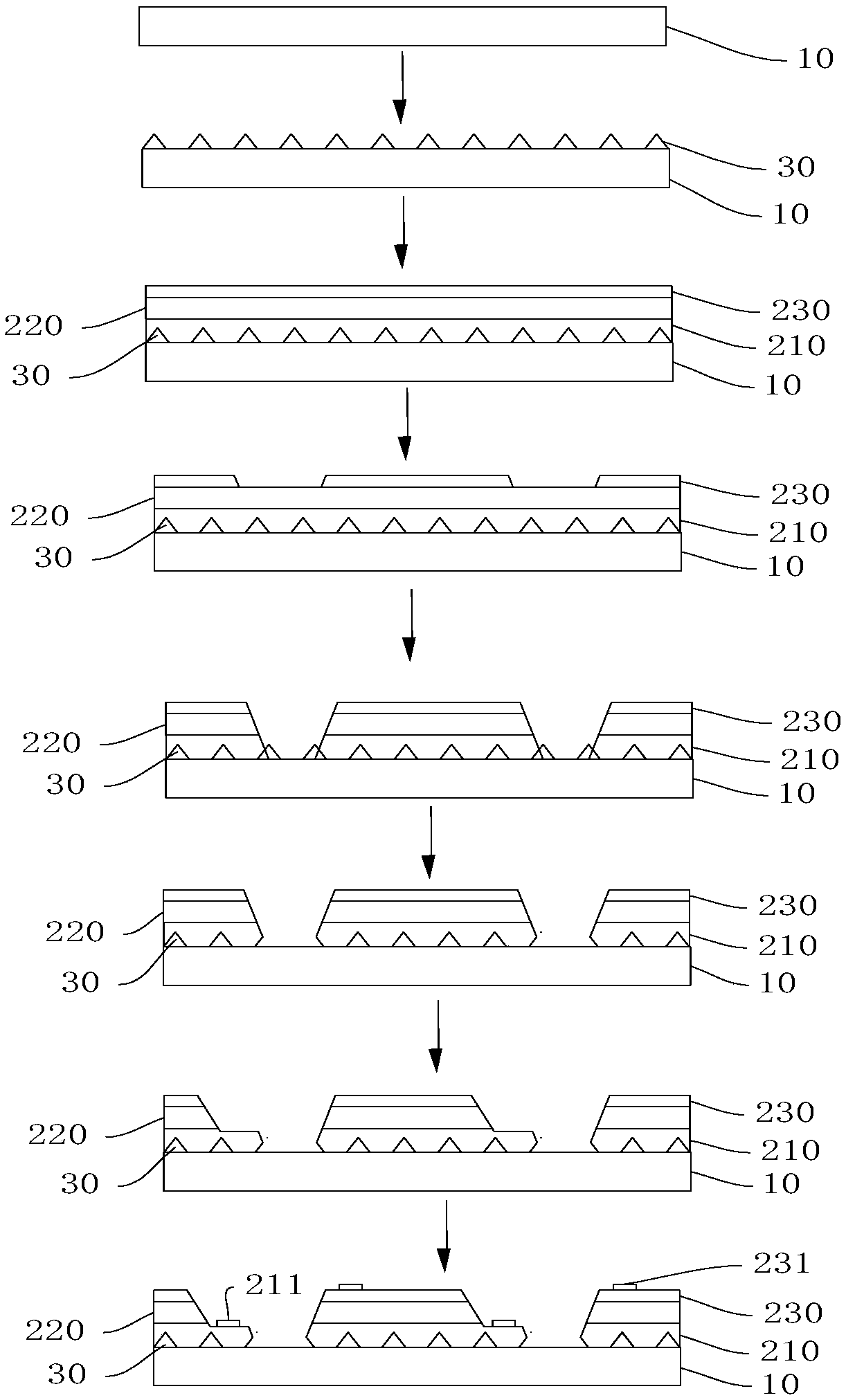
[0034] In order to make the purpose, technical solution and advantages of the present application clearer, the light-emitting diode chip of the present application and its preparation method will be further described in detail through the following examples and in conjunction with the accompanying drawings. It should be understood that the specific embodiments described here are only used to explain the present application, not to limit the present application.

[0035] The light emitting diode chip and the manufacturing method thereof in the embodiments of the present application will be described in detail below with reference to the accompanying drawings.

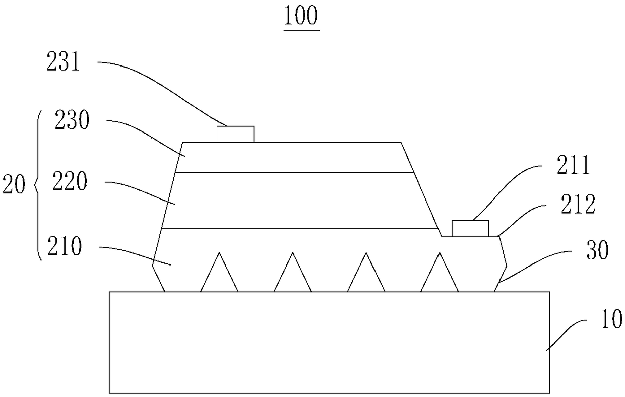
[0036] Please see attached Figure 1-4 , in one embodiment, the preparation method of described LED chip, comprises:

[0037] S100, providing a substrate 10;

[0038] S200, preparing convex structures 30 arranged at intervals on the surface of the substrate 10 through a yellow light process;

[0039] S300, growing an ...


PUM


Abstract

A light emit diode chip and a manufacturing method thereof are provided. The preparation method of the light emitting diode chip comprises the following steps. As a first step, a substrate is provided. 2, prepare a plurality of convex structures on that surface of the substrate by a yellow light proces. 3, grow an epitaxial layer perpendicular to that surface of the substrate to cover the plurality of convex structures. The epitaxial layer includes a first semiconductor layer, an active layer, and a second semiconductor layer, and the first semiconductor layer encloses the convex structure. Fourth, a pattern to be etched is prepared by a photolithography method. 5, etch that epitaxial layer along the pattern to be etch by dry etching to form a plurality of light emitting diode chips arrange at intervals, and exposing the convex structure between adjacent light emitting diode chips. Sixth, removing the convex structure between the plurality of spaced-apart light emitting diode chips bywet etching.

Description

technical field [0001] The present application relates to the field of light emitting diodes, in particular to a light emitting diode chip and a preparation method thereof. Background technique [0002] As an energy-saving, environmentally friendly and low-carbon luminescent material, LED has incomparable advantages compared with traditional lighting. However, in order to completely replace other light sources in the field of lighting, LEDs still need to solve many problems such as unsatisfactory light efficiency, high cost, reducing chip heat generation, and improving LED service life, all of which are restricted by the quantum efficiency of LEDs. The light extraction efficiency of an LED refers to the number of photons generated inside the component that can actually be measured outside the component after being absorbed, refracted, and reflected by the component itself. It can be seen that the factors affecting the extraction efficiency also include the absorption of the...

Claims


Application Information

Patent Timeline
Patent Type & Authority Applications(China)
IPC IPC(8): H01L33/24H01L33/02H01L33/00
CPCH01L33/005H01L33/02H01L33/24
Inventor 刘珊珊宋林青廖汉忠陈顺利丁逸圣
Owner ELEC TECH PHOTOELECTRIC TECH DALIAN
Why Eureka
Try Eureka