A kind of oled display panel and preparation method thereof

A display panel and substrate technology, which is applied in the field of OLED display panels, can solve the problems of backlight transmittance influence, unfavorable light output, large light loss, etc., and achieve the effects of improving color, reducing light loss, and reducing light output efficiency.

Active Publication Date: 2021-08-03
SHENZHEN CHINA STAR OPTOELECTRONICS SEMICON DISPLAY TECH CO LTD
View PDF0 Cites 0 Cited by
  • Summary
  • Abstract
  • Description
  • Claims
  • Application Information

AI Technical Summary

Problems solved by technology

Under such film thickness conditions, the transmittance of the backlight source will be greatly affected, and the light loss will be large, which is not conducive to the final light output.

Method used


Image

  • A kind of oled display panel and preparation method thereof
  • A kind of oled display panel and preparation method thereof
  • A kind of oled display panel and preparation method thereof

Examples


Embodiment Construction

[0031] The technical solution of an OLED display panel and its manufacturing method involved in the present invention will be further described in detail with reference to the accompanying drawings and embodiments.

[0032] The invention relates to an OLED display panel, which comprises a substrate, a light-emitting layer and a color filter layer arranged on the substrate.

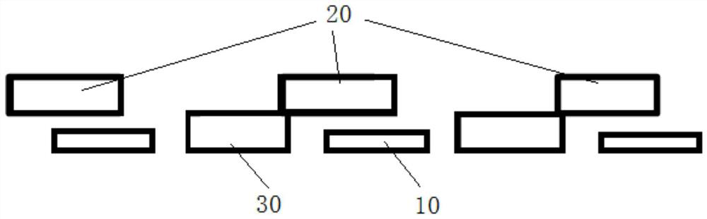
[0033] Such as figure 1 As shown, the light-emitting layer is provided with pixel units 10 arranged at intervals, and the position of the color filter layer corresponding to the pixel unit 10 is provided with a color-resist layer 20 corresponding to the color of the pixel unit. Adjacent colors A BM layer 30 is disposed between the resistance layers 20 . Wherein the thickness of the color filter layer is in the range of 0.1-10um.

[0034] Such as figure 1 As shown in , wherein at least part of the surface area of ​​the pixel unit 10 is exposed from the corresponding color resist layer 20 disposed there...


PUM


Abstract

The invention provides an OLED display panel, which includes a substrate, a light-emitting layer and a color filter layer arranged on the substrate. Wherein the light-emitting layer is provided with pixel units arranged at intervals, and the position of the color filter layer corresponding to the pixel units is provided with a color-resist layer corresponding to the color of the pixel units. Wherein at least part of the surface area of ​​the pixel unit is exposed outside the corresponding color resist layer disposed thereon. That is, the downward projection of the color-resist layer cannot completely cover the surface of the corresponding pixel unit, so that the light emitted from a part of the surface area of ​​the pixel unit can be directly emitted without passing through the color-resist layer. The invention provides an OLED display panel, which adopts a novel color filter layer structure, and the color filter layer can change the color of the backlight without significantly reducing the light transmittance, thus reducing unnecessary light loss.

Description

technical field [0001] The invention relates to the technical field of OLED display panels, in particular, an OLED display panel and a preparation method thereof. Background technique [0002] It is known that display technology has been widely used in production and life, from small-sized and high-resolution wearable VR / AR devices to large-sized and high-brightness outdoor displays, from flat-panel displays to curved displays and then to stereoscopic displays. Apps are everywhere. [0003] At present, the most widely used technology is liquid crystal display (LCD), but the later developed organic light-emitting diode (OLED) display technology is rapidly developing and being applied due to its own advantages. In these two display technologies, the color filter (Color Filter, CF) layer is an indispensable key component. [0004] The most common scenario is that the color film is responsible for converting white light into the three primary colors of red, green, and blue, an...

Claims


Application Information

Patent Timeline
Patent Type & Authority Patents(China)
IPC IPC(8): H01L27/32H01L51/56
CPCH10K59/38H10K71/00
Inventor 李祥龙孟鸿
Owner SHENZHEN CHINA STAR OPTOELECTRONICS SEMICON DISPLAY TECH CO LTD
Why Eureka
Try Eureka