Tunable narrow linewidth external cavity semiconductor laser

A laser and semiconductor technology, applied in the field of lasers, can solve the problems of changes in coupling efficiency, cumbersome tuning process, affecting wavelength tuning and line width narrowing stability, etc. Effect

Inactive Publication Date: 2019-01-04
INST OF SEMICONDUCTORS - CHINESE ACAD OF SCI
View PDF4 Cites 6 Cited by
  • Summary
  • Abstract
  • Description
  • Claims
  • Application Information

AI Technical Summary

Problems solved by technology

This method can achieve a wide range of wavelength tuning and has the effect of narrowing the linewidth, but the position of the diffraction grating in this structure is easily affected by temperature and vibration, which affects the stability of wavelength tuning and linewidth narrowing
There is also a method to lock the optical frequency in the F-P cavity, which is based on the optical heterodyne frequency stabilization technology of the phase modulator. This technology has a good signal-to-noise ratio and a large tuning range, but the tuning process is cumbersome, and the F-P cavity is easy. Influenced by temperature changes and mechanical vibrations
A tunable laser whose external cavity is a fiber grating or a volume grating, changes the reflection peak by changing the temperature of the external grating, and realizes the feedback of light of different wavelengths, thereby realizing wavelength tuning. However, due to the temperature control of the volume grating and the temperature control of the gain chip Not on the same heat sink, during the adjustment process, the optical axis of the volume grating and the gain chip may be misaligned, resulting in changes in coupling efficiency and affecting the stability of the laser

Method used


Image

  • Tunable narrow linewidth external cavity semiconductor laser
  • Tunable narrow linewidth external cavity semiconductor laser

Examples


Embodiment Construction

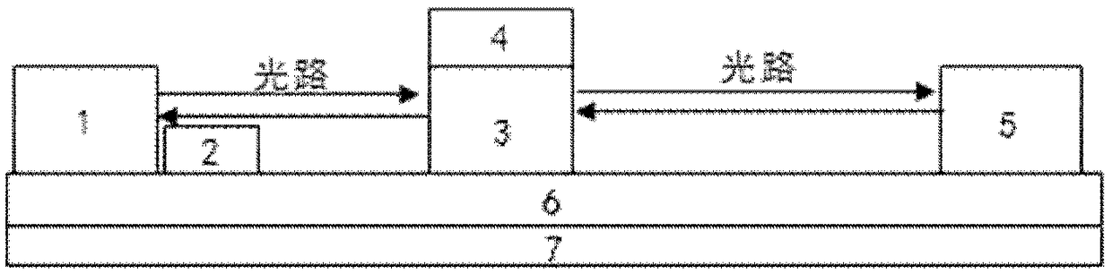
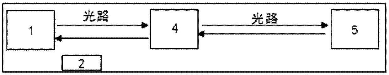
[0033] In order to make the object, technical solution and advantages of the present invention clearer, the present invention will be further described in detail below in conjunction with specific embodiments and with reference to the accompanying drawings. Embodiments of the present invention are described below through specific examples, and those skilled in the art can easily understand other advantages and effects of the present invention from the content disclosed in this specification. It should only be noted that the following drawings are simplified schematic diagrams, and the number, shape and size of the components in the drawings can be changed at will according to the actual implementation situation, and the layout of the components can be more complicated. The present invention can also be implemented or applied through other different specific embodiments, and various modifications and changes can be made to the details in this specification based on different vie...


PUM


Abstract

The invention discloses a tunable narrow linewidth external cavity semiconductor laser, comprising: a semiconductor gain chip as a laser source; An optical waveguide located on the same optical axis as the gain chip; A grating structure positioned behind the optical waveguide and positioned on the same optical axis as the gain chip and the optical waveguide; A thermistor located on one side of thegain chip and the optical waveguide centerline, avoiding the optical path, the thermistor being located close to the gain chip; An electrode attached to the optical waveguide; A heat sink, a gain chip, a thermistor, an optical waveguide and a grating structure are placed on the same heat sink; A heat sink is placed on the same semiconductor cooling sheet. The invention solves the problems of wavelength jitter and linewidth instability caused by external environment and injection current fluctuation of external cavity laser, thereby realizing accurate control of wavelength and linewidth, and realizing rapid adjustment of wavelength.

Description

technical field [0001] The invention relates to the technical field of lasers, in particular to a tunable narrow-linewidth external-cavity semiconductor laser technology. Background technique [0002] Tunable narrow linewidth lasers are widely used in coherent optical communication, laser radar, precision interferometry, dense wavelength division multiplexing, gas concentration detection and other fields. The wavelength tuning speed, wavelength tuning range and light wave linewidth are the key factors of laser performance Important indicators. [0003] Since the laser is very sensitive to fluctuations in operating temperature and injection current, the wavelength of the output light will fluctuate. By optimizing the temperature control circuit and current injection system, it can play a certain role in frequency stabilization, but the linewidth and stability of the laser output light Can not meet the requirements of the above applications. [0004] External cavity lasers a...

Claims


Application Information

Patent Timeline
Patent Type & Authority Applications(China)
IPC IPC(8): H01S5/0687H01S5/14
CPCH01S5/141H01S5/0687
Inventor 陈伟班德超齐艺超祝宁华
Owner INST OF SEMICONDUCTORS - CHINESE ACAD OF SCI
Why Eureka
Try Eureka