
Clock driver circuit

A technology of clock drive and circuit, which is applied in the direction of electrical components, generating electric pulses, amplifiers with semiconductor devices/discharge tubes, etc., can solve the problems of increasing power consumption and scale of circuits, and achieve the expansion of amplitude range, large amplitude, and The effect of increasing the slew rate

Active Publication Date: 2019-01-01
中电科芯片技术(集团)有限公司
View PDF5 Cites 6 Cited by
  • Summary
  • Abstract
  • Description
  • Claims
  • Application Information

AI Technical Summary

Problems solved by technology

[0009] In view of the above-mentioned shortcomings of the prior art, the purpose of the present invention is to provide a clock drive circuit, which is used to solve the problem that the drive circuit in the prior art needs to increase the power consumption and scale of the circuit when reducing the clock jitter

Method used


Image

  • Clock driver circuit
  • Clock driver circuit
  • Clock driver circuit

Examples


Embodiment Construction

[0028] Embodiments of the present invention are described below through specific examples, and those skilled in the art can easily understand other advantages and effects of the present invention from the content disclosed in this specification. The present invention can also be implemented or applied through other different specific implementation modes, and various modifications or changes can be made to the details in this specification based on different viewpoints and applications without departing from the spirit of the present invention. It should be noted that, in the case of no conflict, the following embodiments and features in the embodiments can be combined with each other.

[0029] It should be noted that the diagrams provided in the following embodiments are only schematically illustrating the basic ideas of the present invention, and only the components related to the present invention are shown in the diagrams rather than the number, shape and shape of the compo...


PUM


Abstract

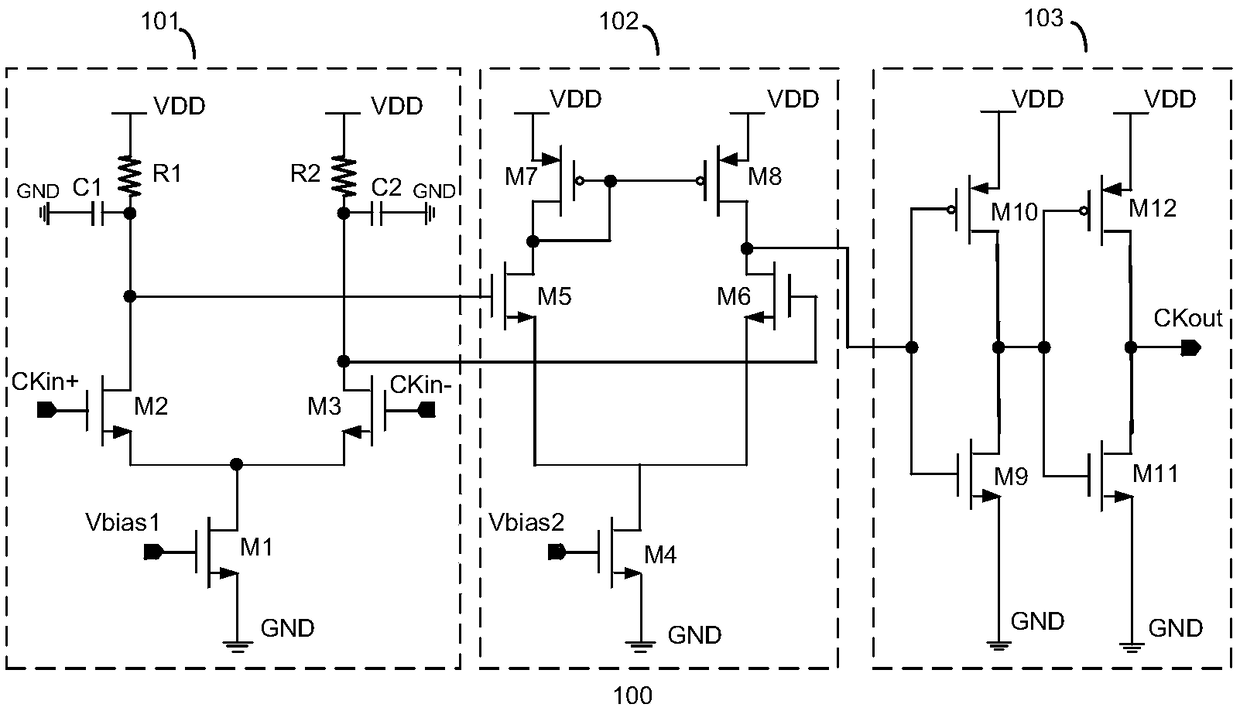
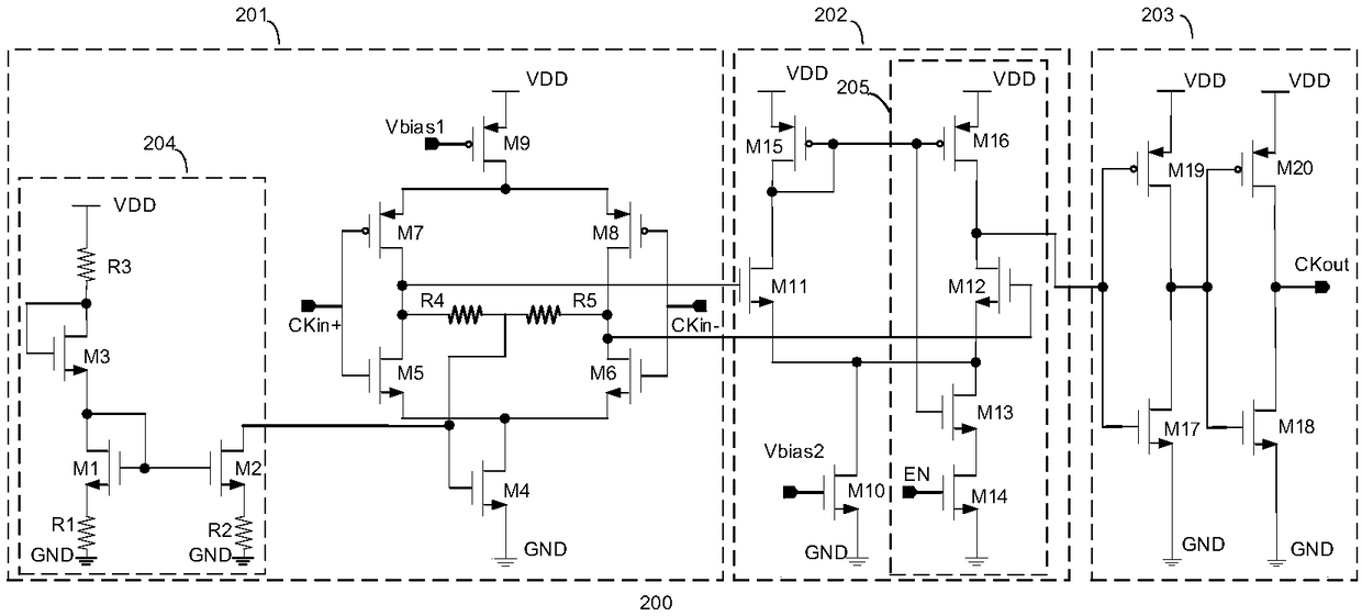
The invention provides a clock driver circuit. The clock driver circuit comprises successively connected input stage, double-end-to-single-end stage and driving output stage, wherein the input stage includes differential amplifiers which are the load for each other and a common mode negative feedback loop; the differential amplifiers access differential clock signals for amplification to generatea common mode voltage; the common mode feedback loop is connected to the output ends of the differential amplifiers for stabilizing the output amplitude of the common mode voltage; the double-end-to-single-end stage converts a differential sinusoidal clock signal outputted by the double-end common mode voltage into a single-end square wave clock signal; and the driving output stage includes a multi-stage-cascaded push-pull inverter, so as to increase the driving capability of the square wave clock signal. The clock driver circuit adopts differential amplifiers which are the load for each other, and any one of the two differential amplifiers acts as the load for the other, thus expanding the amplitude range of the input stage, has the capability of inhaling and supplying a large current, and improves the slew rate, so that the clock driver circuit can receive input clock signals with large amplitude and high speed.

Description

technical field [0001] The invention relates to the technical field of integrated circuits, in particular to a clock drive circuit with low jitter and high speed, which can be applied to data converters in integrated circuits with high requirements for clock circuits. Background technique [0002] With the development of high-speed and high-precision converters, the A / D converters that can realize direct high-frequency sampling have higher and higher requirements on the performance of the clock. Among them, jitter is the most important parameter in the design of the clock drive circuit. The jitter of a clock is defined as the short-term variation of a clock signal from the ideal time position at the threshold level of its logic state change. In high-speed A / D converters, the timing error caused by clock jitter often limits the maximum transmission rate of the digital I / O interface, increases the bit error rate of the signal path, and limits the dynamic range of the analog-to...

Claims


Application Information

Patent Timeline
IPC IPC(8): H03K3/013H03K3/012H03F3/45H03F3/68
CPCH03F3/45636H03F3/68H03K3/012H03K3/013H03F3/45183H03F3/45237H03F3/4565H03F3/3022H03F3/45269
Inventor 沈晓峰黄兴发李梁陈玺徐鸣远王健安付东兵陈光炳
Owner 中电科芯片技术(集团)有限公司
Learn More