Method for manufacturing display panel in mixing and cutting mode, and display panel

A display panel and display device technology, applied in nonlinear optics, instruments, optics, etc., can solve the problem of not being able to take into account the differences in manufacturing processes, not being suitable for display panel integration, and not conducive to improving the mixed cutting technology of high-generation panels, etc. problem, to achieve the effect of improving flexibility

Active Publication Date: 2019-01-01
SHENZHEN CHINA STAR OPTOELECTRONICS TECH CO LTD
View PDF5 Cites 3 Cited by
  • Summary
  • Abstract
  • Description
  • Claims
  • Application Information

AI Technical Summary

Problems solved by technology

In the existing mixed cutting scheme, the manufacturing process of display panels of different sizes is exactly the same, which cannot be applied to the integration of display panels with different manufacturing process requirements
For example, in the production of the color resist layer, there are currently only two cases. The first case is to form the color resist layer only on the lower substrate, and the second case is to form the color resist layer only on the upper substrate, and finally form each The positions of the color-resist layers of display panels of different sizes are exactly the same, so the mixed cutting scheme cannot take into account the differences in the manufacturing process, which is not conducive to improving the mixed cutting technology of high-generation panels

Method used


Image

  • Method for manufacturing display panel in mixing and cutting mode, and display panel
  • Method for manufacturing display panel in mixing and cutting mode, and display panel
  • Method for manufacturing display panel in mixing and cutting mode, and display panel

Examples


Embodiment Construction

[0037] In order to make the object, technical solution and advantages of the present invention more clear, the present invention will be further described in detail below in conjunction with the accompanying drawings and embodiments. It should be understood that the specific embodiments described here are only used to explain the present invention, not to limit the present invention.

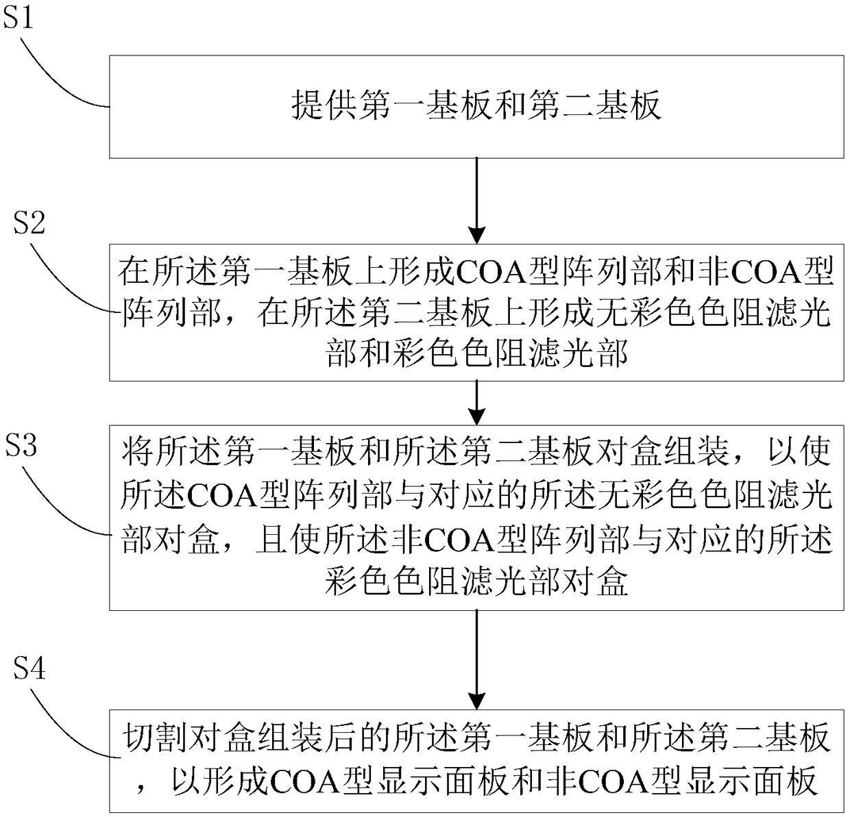
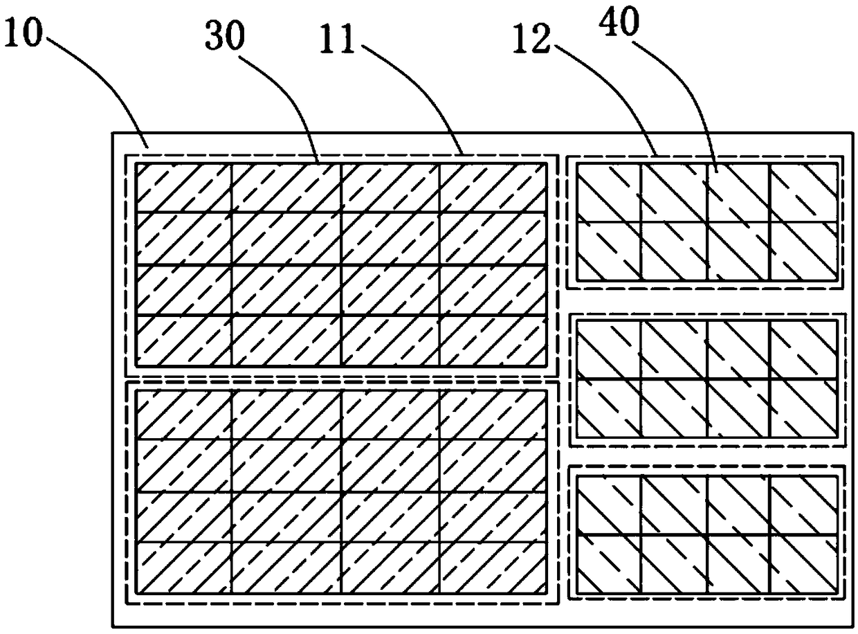
[0038] With the development of high-generation panel technology, in order to improve the utilization rate of glass substrates, the current general mixed-cutting scheme in the industry is to manufacture sub-display panels of different sizes on the same large-size glass substrate, and then cut them to obtain Panels of various sizes. The display panels mentioned below in this embodiment are all uncut display panels integrating multiple sub-display panels of different sizes, and the types of display panels include but are not limited to liquid crystal display panels and OLED display panels.

[0039...


PUM


Abstract

The invention discloses a method for manufacturing a display panel in a mixing and cutting mode and the display panel. The method comprises the steps of providing a first substrate and a second substrate; forming a COA-type array part and a non-COA-type array part on the first substrate, and forming a neutral color color-resistance light-filtering part and a colorful color-resistance light-filtering part on the second substrate; assembling the first substrate and the second substrate in a box pairing mode, so that the COA-type array part and the corresponding neutral color color-resistance light-filtering part are arranged in a box pairing mode, and the non-COA type array part and the corresponding colorful color-resistance light-filtering part are arranged in a box pairing mode; and cutting the first substrate and the second substrate which are assembled in a box pairing mode, so as to form a COA type display panel and a non-COA type display panel. The method for manufacturing the display panel in the mixing and cutting mode can be compatible with the difference of the color resistance process technology in the mixing and cutting scheme, and the flexibility of the mixing and cutting technology is improved.

Description

technical field [0001] The invention belongs to the field of display panel manufacturing, and in particular relates to a method for manufacturing a display panel by mixed cutting and a display panel. Background technique [0002] With the development of high-generation liquid crystal display panel manufacturing technology, the mixed cutting scheme has become an effective way to improve the utilization rate of the panel. The so-called mixed cutting scheme is to prepare display panels of two or more sizes on the same glass substrate. In the existing mixed cutting solution, the manufacturing processes of display panels of different sizes are completely consistent, which cannot be applied to the integration of display panels with different manufacturing process requirements. For example, in the manufacture of the color-resist layer, there are currently only two cases. The first case is to form the color-resist layer only on the lower substrate, and the second case is to form the...

Claims


Application Information

Patent Timeline
IPC IPC(8): G02F1/1333
CPCG02F1/133351
Inventor 杨帆徐向阳
Owner SHENZHEN CHINA STAR OPTOELECTRONICS TECH CO LTD
Why Eureka
Try Eureka