Liquid crystal display panel and preparation method thereof

A technology of liquid crystal display panels and array substrates, applied in nonlinear optics, instruments, optics, etc., can solve the problems of being unable to act as a barrier, unable to make a raised barrier, and unable to have a barrier, so as to avoid pollution Effect

Active Publication Date: 2018-12-18
SHENZHEN CHINA STAR OPTOELECTRONICS SEMICON DISPLAY TECH CO LTD
View PDF5 Cites 3 Cited by
  • Summary
  • Abstract
  • Description
  • Claims
  • Application Information

AI Technical Summary

Problems solved by technology

Since there is no patterned film layer on the side of the color filter substrate, there is no design for retaining walls
The BPS material layer on the side of the array substrate acts as a light-shielding function, so it is impossible to make a raised barrier, and it cannot be realized even if a color resist is used as a barrier, because the planarization layer and the BPS material layer are both organic layers, and both It is very thick, so the bumps of the color resistance will be flattened by the two organic layers, and cannot function as a barrier

Method used


Image

  • Liquid crystal display panel and preparation method thereof
  • Liquid crystal display panel and preparation method thereof
  • Liquid crystal display panel and preparation method thereof

Examples


Embodiment Construction

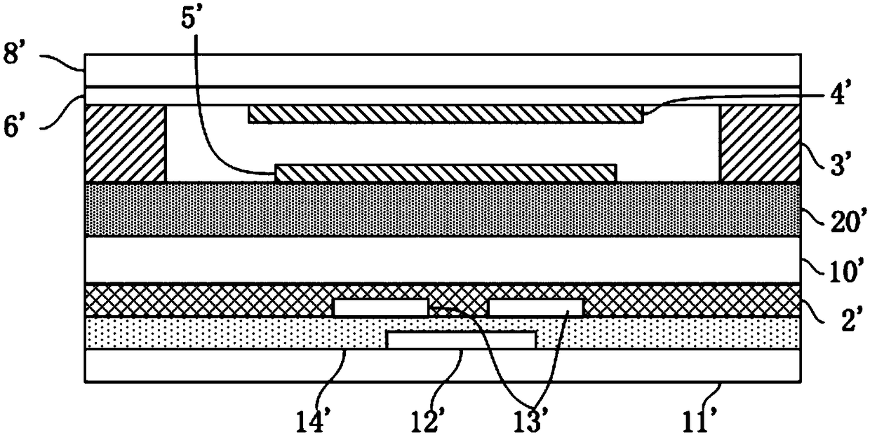
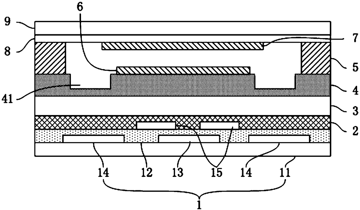
[0033] The invention provides a liquid crystal display panel, such as image 3 The liquid crystal display panel shown includes: an array substrate 1, a passivation layer 2, a planarization layer 3, a BPS (Black photo spacer, black photoresist pad material) material layer 4 sequentially stacked on the array substrate 1, and a first alignment layer 6 , the projection of the first alignment layer 6 on the BPS material layer 4 does not exceed the area of ​​the BPS material layer 4 . The material of the alignment layer is polyimide material.

[0034] Such as Figure 4 As shown, a plurality of grooves 41 are provided on the BPS material layer 4, and the plurality of grooves 41 are distributed along the inner side of the edge of the BPS material layer 4, and a frame glue 5 is also formed on the BPS material layer 4; wherein, The sealant 5 and the first alignment layer 6 are respectively located on two sides of the plurality of grooves 41 .

[0035] Here, since the BPS material lay...


PUM


Abstract

The invention provides a liquid crystal display panel and a preparation method thereof. The liquid crystal display panel comprises an array substrate, a passivation layer, a planarization layer, a BPSmaterial layer and a first orientation layer, wherein the passivation layer, the planarization layer, the BPS material layer and the first orientation layer are sequentially stacked on the array substrate; the projection of the first orientation layer on the BPS material layer does not exceed the area of the BPS material layer; and multiple grooves are formed in the BPS material layer and distributed along the inner side of the edge of the BPS material layer, and a frame adhesive is formed on the BPS material layer, wherein the frame adhesive and the first orientation layer are located at thetwo sides of the multiple grooves respectively. According to the liquid crystal display panel and the preparation method thereof, flowing of the frame adhesive and the first orientation layer can bestopped without preparing a stop wall on the array substrate, and the situation that the frame adhesive and the first orientation layer on the array substrate exceed specifications in preparation is avoided.

Description

technical field [0001] The invention relates to the field of display technology, in particular to a liquid crystal display panel and a preparation method thereof. Background technique [0002] BPS (Black photo spacer, black photoresist spacer material) technology is a technology in LCD (Liquid Crystal Display, liquid crystal display) technology that combines two processes of BM (black matrix) and PS (gap control) into one process. This technology can perform BPS process on the color filter substrate side or array substrate side, perform BPS process on the array substrate side, and then use COA (Color on Array, integrating color filter substrate and array substrate together) technology to integrate the array substrate and color filter The substrate is assembled into a box, and the corresponding color filter substrate side has only one front ITO (indium tin oxide) electrode layer, and there are no other film layers. This design can be applied to the situation where the flat d...

Claims


Application Information

Patent Timeline
IPC IPC(8): G02F1/1339G02F1/1343G02F1/1337G02F1/1333
CPCG02F1/1333G02F1/1337G02F1/1339G02F1/13439
Inventor 叶岩溪
Owner SHENZHEN CHINA STAR OPTOELECTRONICS SEMICON DISPLAY TECH CO LTD
Why Eureka
Try Eureka