
To-be-cute display module and manufacturing method thereof

The technology of a display module and manufacturing method, which is applied in the field of panel manufacturing, can solve the problems of poor display effect of the display panel, and achieve the effects of reducing processing time and eliminating dust accumulation

Active Publication Date: 2018-12-18
WUHAN CHINA STAR OPTOELECTRONICS SEMICON DISPLAY TECH CO LTD
View PDF5 Cites 3 Cited by
  • Summary
  • Abstract
  • Description
  • Claims
  • Application Information

AI Technical Summary

Problems solved by technology

[0007] The invention provides a display module to be cut and a manufacturing method thereof, so as to solve the technical problem of poor display effect of the existing display panel

Method used


Image

  • To-be-cute display module and manufacturing method thereof
  • To-be-cute display module and manufacturing method thereof
  • To-be-cute display module and manufacturing method thereof

Examples


Embodiment Construction

[0040] The following descriptions of the various embodiments refer to the accompanying drawings to illustrate specific embodiments in which the invention may be practiced. The directional terms mentioned in the present invention, such as [top], [bottom], [front], [back], [left], [right], [inside], [outside], [side], etc., are only for reference The orientation of the attached schema. Therefore, the directional terms used are used to illustrate and understand the present invention, but not to limit the present invention. In the figures, structurally similar elements are denoted by the same reference numerals.

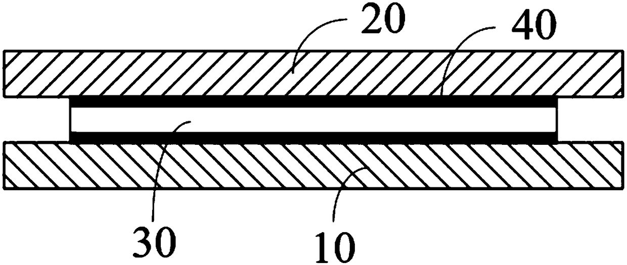
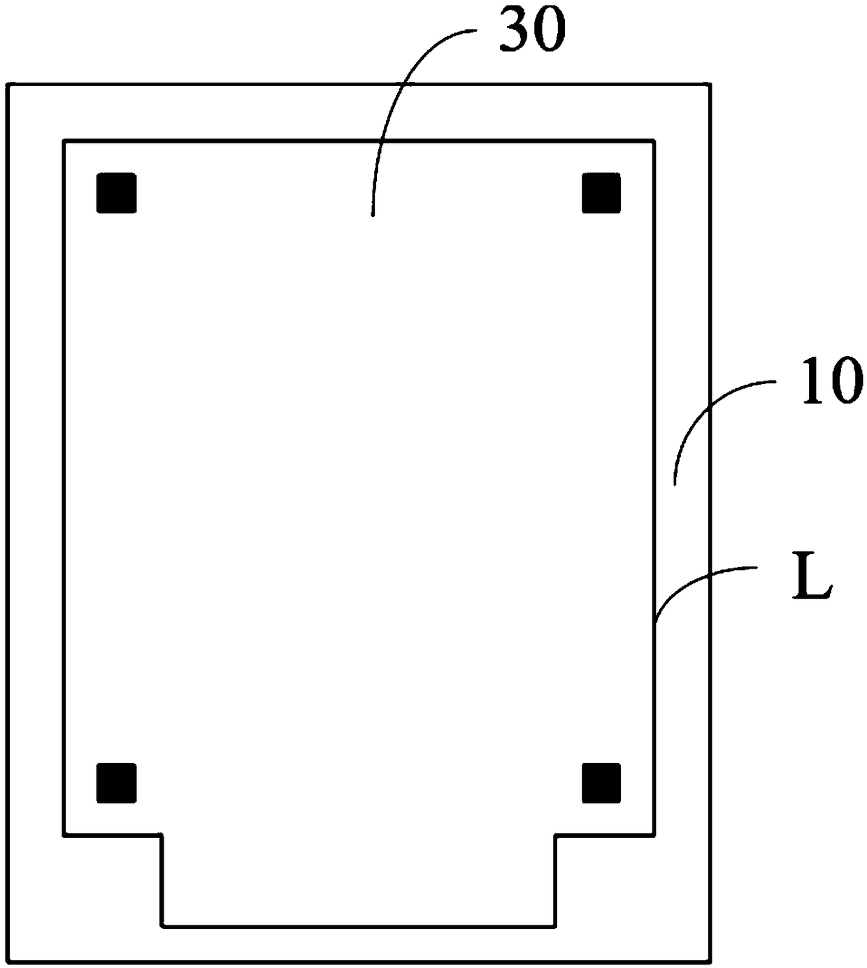
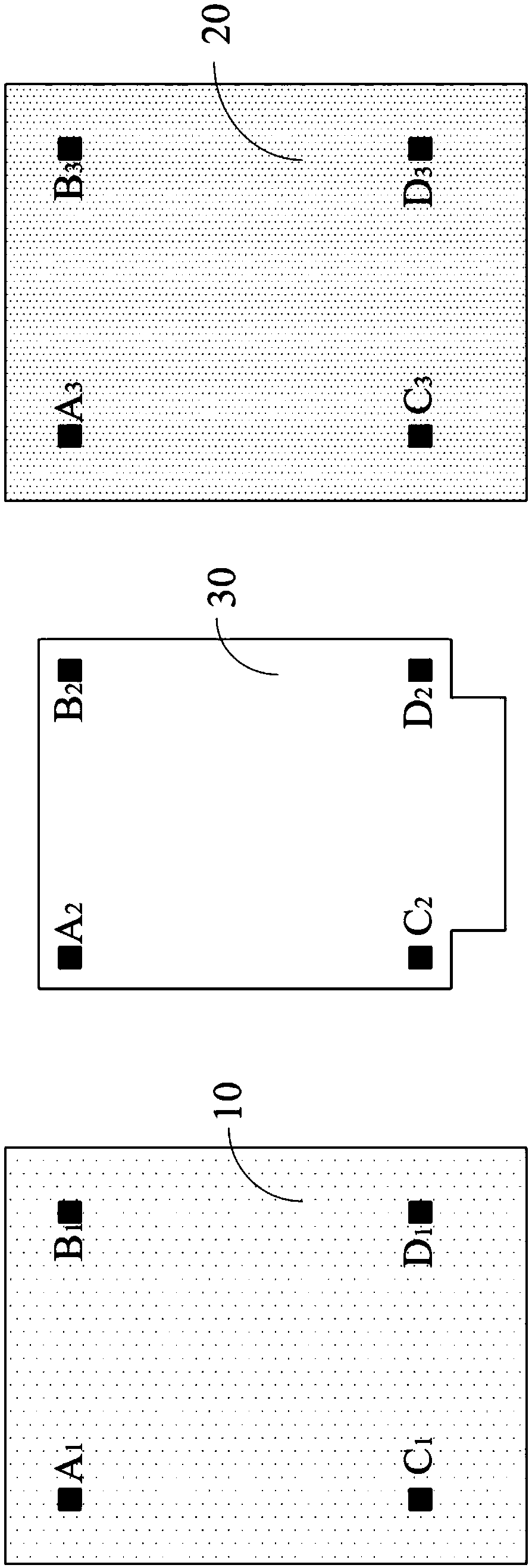
[0041] figure 1 The present invention presents a layer structure diagram of a display module to be cut. The display module to be cut includes a support layer 10 , a display panel 20 and a backplane layer 30 .

[0042] The support layer 10 is located at the base of the display module to be cut, and is mainly used to support the structures on the support layer 10 .

[...


PUM


Abstract

The invention provides a to-be-cut display module and a manufacturing method thereof. The to-be-cut display module comprises a support layer, a display panel located on the support layer, and a backboard layer located between the support layer and the display panel; and a shape of a positive projection of the backboard layer on the display panel is same as the shape of a target display module. Thebackboard layer is arranged as the shape same as that of the target display module, so that a cutting machine processes the to-be-cut display module by taking an outer circle of the backboard layer as a cutting path; the ash deposit on the backboard layer is eliminated, and the processing time is reduced.

Description

technical field [0001] The invention relates to the field of panel manufacturing, in particular to a display module to be cut and a manufacturing method thereof. Background technique [0002] In recent years, the display technology has developed rapidly, and the flat panel display has replaced the heavy CRT (Cathode Ray Tube, cathode ray tube) display and has been deeply involved in people's daily life. Currently, common flat panel displays include LCD (Liquid Crystal Display, liquid crystal display) and OLED (Organic Light-Emitting Diode, organic light-emitting diode) displays. [0003] At present, the display screens of common devices, such as mobile phones, tablet computers or notebook computers, are relatively small, and the cost of display panel photomask process is relatively high; therefore, the display screens of common electronic devices in the prior art are usually made of a larger The display panel is cut and processed. [0004] In the prior art, the display mod...

Claims


Application Information

Patent Timeline
IPC IPC(8): G02F1/1333H01L27/32
CPCG02F1/1333G02F1/133308G02F1/133302G02F1/133314H10K59/88H10K59/00
Inventor 宋月龙
Owner WUHAN CHINA STAR OPTOELECTRONICS SEMICON DISPLAY TECH CO LTD
Learn More