
End face coupler and manufacturing method therefor

A technology of end-face coupling and a buried oxide layer, which is applied in the direction of instruments, light guides, optics, etc., can solve the problems of unfavorable large-scale promotion and application, complex processing of couplers, and incompatibility between preparation technology and CMOS technology, and achieve high industrial efficiency. Use value, low cost, shortened length effect

Active Publication Date: 2018-12-11
南通赛勒光电科技有限公司
View PDF6 Cites 8 Cited by
  • Summary
  • Abstract
  • Description
  • Claims
  • Application Information

AI Technical Summary

Problems solved by technology

In response to this problem, a variety of end face couplers have been proposed in the world to achieve larger mold spot sizes, mainly including cantilever beam structures, coated polymer structures, three-dimensional wedge structures, etc., but these couplers are complicated to process. The preparation process of its corresponding structure is not compatible with the CMOS process, which is not conducive to large-scale promotion and application

Method used


Image

  • End face coupler and manufacturing method therefor
  • End face coupler and manufacturing method therefor
  • End face coupler and manufacturing method therefor

Examples


Embodiment Construction

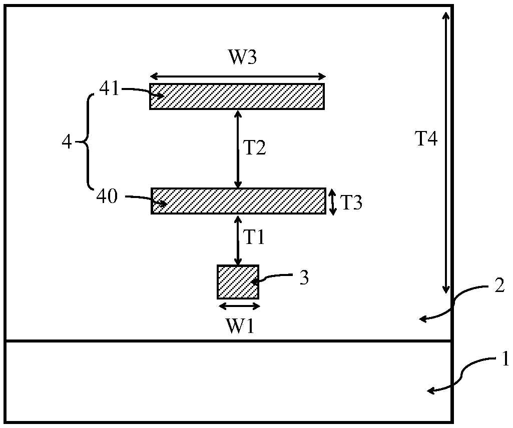
[0048] The following will clearly and completely describe the technical solutions in the embodiments of the present invention with reference to the accompanying drawings in the embodiments of the present invention. Obviously, the described embodiments are only some, not all, embodiments of the present invention. Based on the embodiments of the present invention, all other embodiments obtained by persons of ordinary skill in the art without creative efforts fall within the protection scope of the present invention.

[0049] It should be noted that, in the case of no conflict, the embodiments of the present invention and the features in the embodiments can be combined with each other.

[0050] The present invention will be further described below in conjunction with the accompanying drawings and specific embodiments, but not as a limitation of the present invention.

[0051] The present invention includes an end face coupler comprising:

[0052] A silicon substrate 1;

[0053]...


PUM

PropertyMeasurementUnit
conversion efficiencyaaaaaaaaaa
refractive indexaaaaaaaaaa

Abstract

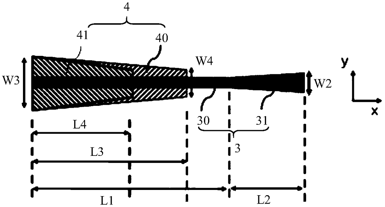
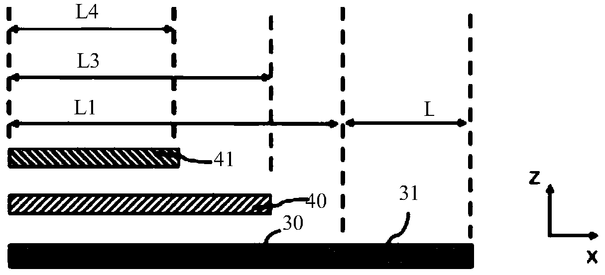
The invention discloses an end face coupler and a preparation method therefor, and the coupler comprises a silicon substrate; a buried oxide layer which is formed on an upper surface of the silicon substrate; top silicon which is formed in the buried oxide layer, and has first top silicon and second top silicon; silicon nitride waveguides formed on the top silicon, wherein the silicon nitride waveguides include a first silicon nitride waveguide and a second silicon nitride waveguide, wherein the central lines of the first silicon nitride waveguide and the second silicon nitride waveguide are located on the central line of the top silicon. The beneficial effects are that by growing a plurality of silicon nitride waveguides at different heights above the top silicon, a light field of a largeplaque size is realized, and the length of the longitudinal structure is reduced by combining the design of a longitudinal wedge structure, and finally a waveguide end face coupler with the high coupling efficiency is formed; the end face coupler is simple in fabrication process, is compatible with CMOS process, can be used for mass production, has low cost, and has a high industrial utilizationvalue.

Description

technical field [0001] The invention relates to the technical field of optical devices, in particular to an end face coupler and a preparation method thereof. Background technique [0002] Silicon photonics technology uses silicon as the optical medium, and uses CMOS (Complementary Metal Oxide Semiconductor, English full name Complementary Metal Oxide Semiconductor) technology for the development and integration of optical devices, which is expected to achieve low-cost, high-speed optical communication, and has broad market application prospects . How to efficiently realize the interconnection between the optical signal on the optical chip and the external optical signal has become one of the key technologies in silicon photonics technology. The mode spot size of the silicon-based single-mode waveguide is 0.4-0.5um, while the mode spot size of the single-mode fiber is 9-10um. There is a large mode spot size mismatch and effective refractive index mismatch between the two. ...

Claims


Application Information

Patent Timeline
Patent Type & Authority Applications(China)
IPC IPC(8): G02B6/10G02B6/122G02B6/136
CPCG02B6/10G02B6/122G02B6/136G02B2006/12147
Inventor 柏艳飞仇超甘甫烷
Owner 南通赛勒光电科技有限公司
Learn More