Touch panel, manufacturing method thereof and display device
A technology of a touch panel and a manufacturing method, which is applied in the direction of instruments, electrical digital data processing, and the input/output process of data processing, etc., and can solve problems such as strong reflected light on the screen, and the user cannot see the screen clearly, and the method is simple and convenient Operation, effect of reducing haze
- Summary
- Abstract
- Description
- Claims
- Application Information
AI Technical Summary
Problems solved by technology
Method used
Image
Examples
Embodiment 1
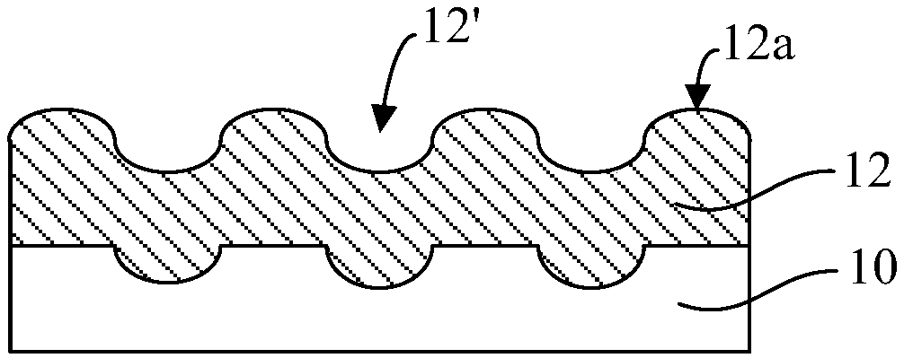
[0039] Please refer to Figure 2b As shown, the touch panel provided in this embodiment includes: a substrate 10 and a nano-metal layer 12 on the substrate 10 , the nano-metal layer 12 has an uneven surface 12 a on a side away from the substrate 10 .
[0040] In this embodiment, the side of the substrate 10 close to the nano-metal layer 12 is also formed with an uneven surface, and the nano-metal layer 12 matches the structure of the adjacent surface of the substrate 10 . In this embodiment, the uneven surface of the substrate 10 corresponds to the position of the concave part in the uneven surface of the nano-metal layer 12, and the uneven surface of the substrate 10 corresponds to the position of the nano-metal layer 12. Corresponds to the depth of the recesses in the uneven surface. Specifically, a plurality of grooves 10' are formed on the side of the substrate 10 close to the nano silver wire layer 12, and the grooves 10' are filled with the nano metal layer 12.
[0041...
Embodiment 2
[0056] Please refer to Figure 3b As shown, the touch panel provided by this embodiment includes: a base 20 and a nano-metal layer 22 on the base 20 , the side of the nano-metal layer 22 away from the base 20 has an uneven surface 22 a.
[0057] In this embodiment, the surface 20a of the substrate 20 close to the nano-metal layer 22 is a flat surface, correspondingly, the surface of the nano-metal layer 22 close to the substrate 20 is also a flat surface, and the nano-metal The surface 22a of the layer 22 away from the substrate 20 is an uneven surface. Specifically, a plurality of grooves 22' are formed on the side of the silver nano wire layer 22 away from the substrate 20.
[0058] The grooves 22' can be evenly distributed in the nano-metal layer 12, and the grooves 22' can also be distributed non-uniformly in the nano-metal layer 12, for example, relatively more slits are distributed in areas with severe haze. grooves, and areas where no haze is present form no or fewer ...
PUM
| Property | Measurement | Unit |
|---|---|---|
| Line length | aaaaa | aaaaa |
Abstract
Description
Claims
Application Information
 - R&D
- Intellectual Property
- Life Sciences
- Materials
- Tech Scout
- Unparalleled Data Quality
- Higher Quality Content
- 60% Fewer Hallucinations
Browse by: Latest US Patents, China's latest patents, Technical Efficacy Thesaurus, Application Domain, Technology Topic, Popular Technical Reports.
© 2025 PatSnap. All rights reserved.Legal|Privacy policy|Modern Slavery Act Transparency Statement|Sitemap|About US| Contact US: help@patsnap.com


