
Surface-enhanced Raman spectroscopy substrate and preparation method and application thereof

A surface-enhanced Raman and substrate technology, applied in the field of Raman spectroscopy, can solve the problems of uneven distribution, poor control of large-area order, low efficiency, etc., to achieve enhanced Raman scattering, rapid large-area production, Craft a simple effect

Inactive Publication Date: 2018-11-16
SOUTH CHINA NORMAL UNIVERSITY
View PDF5 Cites 7 Cited by
  • Summary
  • Abstract
  • Description
  • Claims
  • Application Information

AI Technical Summary

Problems solved by technology

At present, nano-rough surface or periodic nano-structured substrates are mainly used as SERS substrates. The preparation methods include self-assembly method, sol-particle method, electron beam lithography, focused plasma beam etching, etc., but these preparation methods have certain limitations. Limitations, such as rough surface, there are problems of random dispersion and uneven distribution of hot spots; the substrate prepared by the self-assembly method has more defects, and the large-area order is not easy to control; and for electron beam lithography, focused plasma beam lithography If the top-down process such as etching is used, the cost of preparation is too high and the efficiency is too low, so it is difficult to realize large-scale production application
[0004] The above-mentioned problems hinder the further popularization and application of SERS technology, so there is an urgent need for a simple preparation process, low cost, long-term preservation, good periodicity, small gap between nanostructure tips and precise control, random Take the ready-to-use high-efficiency SERS active substrate

Method used


Image

  • Surface-enhanced Raman spectroscopy substrate and preparation method and application thereof
  • Surface-enhanced Raman spectroscopy substrate and preparation method and application thereof
  • Surface-enhanced Raman spectroscopy substrate and preparation method and application thereof

Examples


Embodiment 1

[0037] (1) The silicon substrate is cleaned and hydrophobically treated in sequence: first, the silicon substrate dissociated into a certain size is ultrasonically cleaned in acetone, isopropanol, and deionized water, and then rinsed with deionization and blown dry with nitrogen. Then, a layer of hexamethyldisilazane (HMDS) with a thickness of 5 nanometers is covered on the surface of the silicon substrate by means of steam, so that the surface of the silicon substrate can obtain better hydrophobicity.

[0038] (2) Get the silicon substrate that has been cleaned and treated with hydrophobicity, place it in a homogenizer with a rotating speed of 4000rpm, and add an appropriate amount of AR-P3740 positive photoresist (produced by Allresist, Germany) dropwise on the silicon substrate. After the bottom surface was spin-coated for 45 seconds, it was taken out and baked at 90° C. for 2 minutes, and the average thickness of the obtained photoresist was 300 nm.

[0039] (3) First, usi...


PUM

PropertyMeasurementUnit
The average thicknessaaaaaaaaaa
Thicknessaaaaaaaaaa

Abstract

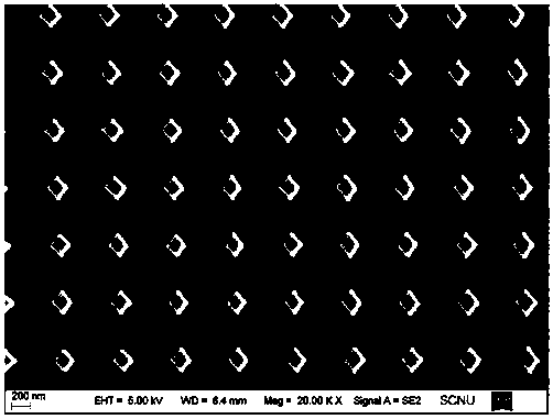
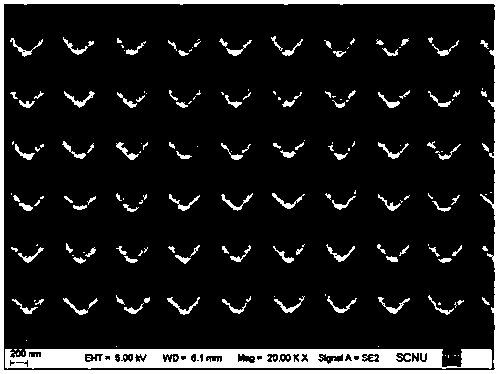
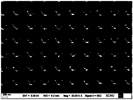
The invention provides a surface-enhanced Raman spectroscopy substrate and a preparation method and application thereof. The method comprises the following steps: performing cleaning and hydrophobic treatment to silicon substrate in sequence; forming a polymer layer on the silicon substrate; carving on the polymer layer with ultraviolet laser interference light to form a nanometer square array structure; using inducing coupling plasma to etch the nanometer square array structure of the polymer layer to transfer and form a silicon nanometer square structure; plating a metal active layer on thesilicon nanometer square structure to obtain the SERS ( surface-enhanced Raman spectroscopy) substrate. The method provided by the invention has the advantages of simple and convenient process and lowcost; the SERS substrate can be prepared quickly in a large-area manner; besides, the endpoint of a periodic gold nanometer square structure on the SERS substrate is sharp, and the clearance betweenthe tips of the structure is controllable, so that Raman signals can be enhanced advantageously; and the method is very suitable for mass production and application.

Description

technical field [0001] The invention belongs to the technical field of Raman spectroscopy, in particular to a surface-enhanced Raman scattering substrate, a preparation method and an application. Background technique [0002] Surface-enhanced Raman scattering (SERS) technology is a method of material structure analysis that does not require labeling of test samples. It has the advantages of high sensitivity, high accuracy, and non-destructive testing. It is used in biochemistry, material composition identification, and food safety. The field has great application potential. [0003] The advantages of SERS technology are very clear, and the preparation of high-performance and practical SERS active substrates is one of the important prerequisites for the realization of SERS detection. At present, nano-rough surface or periodic nano-structured substrates are mainly used as SERS substrates. The preparation methods include self-assembly method, sol-particle method, electron beam...

Claims


Application Information

Patent Timeline
IPC IPC(8): G01N21/65
CPCG01N21/658
Inventor 杨军星张渊胡治朋黄广飞
Owner SOUTH CHINA NORMAL UNIVERSITY
Learn More