An Enhancement Mode High Electron Mobility Transistor with High Threshold Voltage

A high electron mobility, high threshold voltage technology, applied in circuits, electrical components, semiconductor devices, etc., can solve problems such as low threshold voltage, and achieve the effect of increasing the threshold voltage and the conduction band energy level

Active Publication Date: 2021-08-03
SOUTHEAST UNIV
View PDF0 Cites 0 Cited by
  • Summary
  • Abstract
  • Description
  • Claims
  • Application Information

AI Technical Summary

Problems solved by technology

[0008] Purpose of the invention: To solve the problem of low threshold voltage of the enhanced HEMT device prepared by the above-mentioned prior art, the present invention provides a novel enhanced high electron mobility transistor with high threshold voltage

Method used


Image

  • An Enhancement Mode High Electron Mobility Transistor with High Threshold Voltage
  • An Enhancement Mode High Electron Mobility Transistor with High Threshold Voltage
  • An Enhancement Mode High Electron Mobility Transistor with High Threshold Voltage

Examples


Embodiment 1

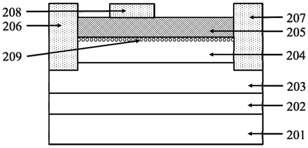
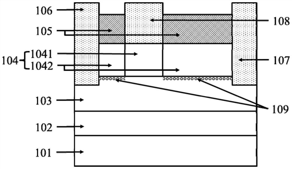
[0024] image 3 An enhanced HEMT with a high threshold voltage provided by the present invention, a sapphire substrate (101), an AlN buffer layer (102), a non-doped GaN layer (103), and an n-type AlGaN layer are sequentially arranged from bottom to top (104) and a silicon nitride passivation layer (105), wherein the n-type AlGaN layer (104) is composed of a nitrogen polarity AlGaN layer (1041) and a metal polarity AlGaN layer (1042). The source (106) and the drain (107) are respectively arranged at both ends of the n-type AlGaN layer (104) and form contact with the non-doped GaN layer (103), and the gate (108) is arranged on the n-type AlGaN layer (104) above.

[0025] The nitrogen polar AlGaN layer (1041) is located directly below the gate (108), has the same width as the gate (108), both 1000 nm, and the same thickness as the metal polar AlGaN layer (1042), both 200 nm .

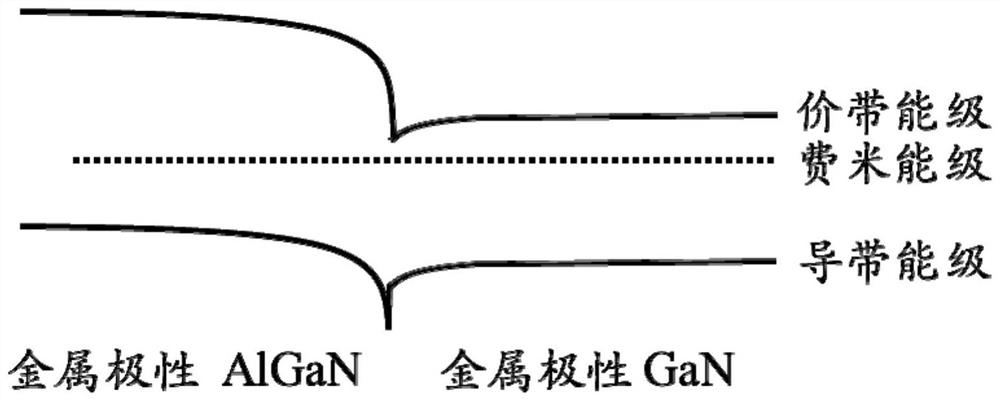
[0026] The introduction of the nitrogen-polar AlGaN layer (1041) can be realized through the followi...


PUM

PropertyMeasurementUnit
thicknessaaaaaaaaaa
thicknessaaaaaaaaaa
thicknessaaaaaaaaaa

Abstract

The invention discloses an enhanced high electron mobility transistor with a high threshold voltage, which comprises a substrate, a buffer layer, a non-doped GaN layer, an n-type AlGaN layer and a passivation layer arranged sequentially from bottom to top, and a source The drain and the drain are respectively arranged at both ends of the n-type AlGaN layer and are in contact with the non-doped GaN layer, and the gate is arranged on the n-type AlGaN layer; the n-type AlGaN layer is composed of a nitrogen polarity AlGaN layer and a metal polarity AlGaN layer. layer composition. The invention realizes a higher threshold voltage by introducing an AlGaN / GaN heterojunction energy band structure composed of a nitrogen polarity AlGaN layer different from the traditional metal polarity GaN layer and a metal polarity GaN layer.

Description

technical field [0001] The invention belongs to the technical field of semiconductor devices, in particular to an enhanced high electron mobility transistor with high threshold voltage. Background technique [0002] GaN-based high electron mobility transistor (HEMT) is a heterojunction field-effect transistor, which uses a two-dimensional electron gas with quantum effects in the heterojunction to form a conductive channel, with wide band gap, high saturation electron mobility, The advantages of high breakdown electric field and high thermal conductivity are widely used in the fields of high frequency, high power, high temperature and high radiation devices. [0003] However, if figure 1 As shown, it is precisely because of the high concentration of two-dimensional electron gas at the interface of the AlGaN / GaN heterojunction that the HEMT device fabricated from it must become a depletion-mode device while having a high saturation electron mobility. , that is, when no bias ...

Claims


Application Information

Patent Timeline
Patent Type & Authority Patents(China)
IPC IPC(8): H01L29/06H01L21/335H01L29/778
CPCH01L29/0684H01L29/66462H01L29/778
Inventor 张雄陈虎吴自力崔一平
Owner SOUTHEAST UNIV
Why Eureka
Try Eureka