Array substrate and manufacturing method and display device thereof

A technology of array substrates and substrate substrates, which is applied in semiconductor/solid-state device manufacturing, optics, instruments, etc., and can solve the problems of low yield rate of array substrates

Active Publication Date: 2018-11-13
BOE TECH GRP CO LTD +1
View PDF13 Cites 13 Cited by
  • Summary
  • Abstract
  • Description
  • Claims
  • Application Information

AI Technical Summary

Problems solved by technology

[0005] The present application provides an array substrate, its manufacturing method, and a display device, which can solve the problem of low yield rate of existing array substrates

Method used


Image

  • Array substrate and manufacturing method and display device thereof
  • Array substrate and manufacturing method and display device thereof
  • Array substrate and manufacturing method and display device thereof

Examples


Embodiment Construction

[0038] In order to make the object, technical solution and advantages of the present invention clearer, the implementation manner of the present invention will be further described in detail below in conjunction with the accompanying drawings.

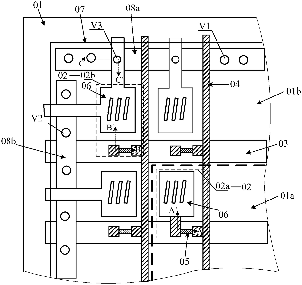
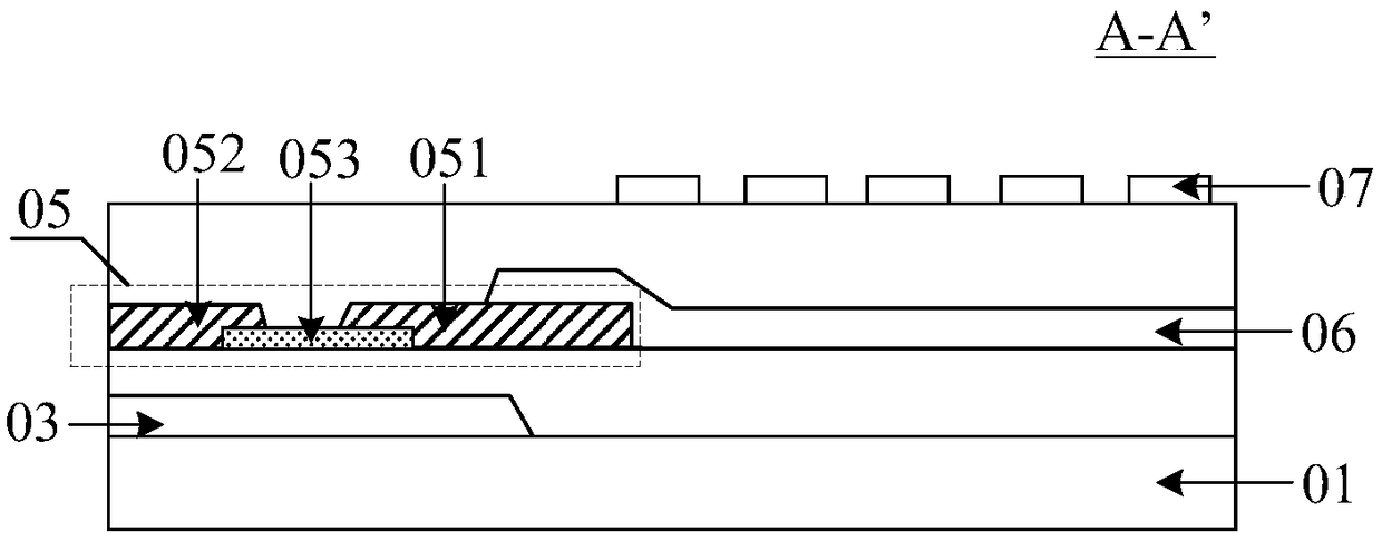
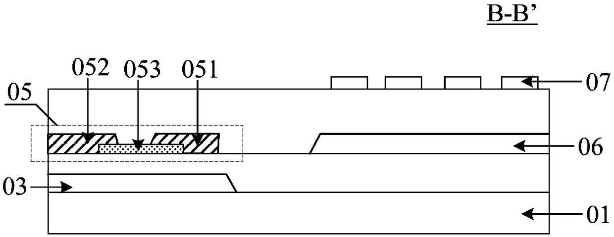
[0039] Please refer to figure 1 , figure 1 It is a top view of an array substrate provided in the related art, and the array substrate includes: a base substrate 01, and the base substrate 01 has a display area 01a and a non-display area 01b.

[0040] The array substrate 01 is provided with a plurality of pixel units 02 , a plurality of gate lines 03 and a plurality of data lines 04 . In the display area 01 a , any two adjacent gate lines 03 and any two adjacent data lines 04 can form a pixel unit 02 .

[0041] The plurality of pixel units 02 includes: a pixel unit 02a located in the display area 01a, and a pixel unit 02b located in the non-display area 01b, and the pixel unit 02b is also called a dummy pixel unit. Usually, a circle...


PUM


Abstract

The invention discloses an array substrate and a manufacturing method and a display device thereof and belongs to the technical field of display. The array substrate comprises a substrate base plate.Multiple virtual pixel units are arranged in a non-display area of the substrate base plate and surround the non-display area of the substrate base plate. The substrate base plate is also provided with multiple parallelly arranged grid lines. The multiple virtual pixel units include multiple first virtual pixel units with the arrangement direction parallel to the extending direction of the grid lines, wherein each first virtual pixel unit comprises a public electrode, a thin film transistor (TFT) and a pixel electrode. In each first virtual pixel unit, the pixel electrode is connected with theTFT, and the pixel electrode is not connected with a public electrode. In each first virtual pixel unit, a first storage capacitor can be formed between the pixel electrode and the public electrode,static electricity can be released in the first storage capacitor, and the possibility is reduced that the TFT in the pixel units are affected by the static electricity and accordingly are invalid inthe display area.

Description

technical field [0001] The present invention relates to the field of display technology, in particular to an array substrate, a manufacturing method thereof, and a display device. Background technique [0002] With the development of display technology, various products with display functions appear in our daily life, such as mobile phones, tablet computers, TVs, notebook computers, digital photo frames and navigators, etc., all of which need to be equipped with display panel. [0003] At present, most display panels may include an array substrate, a color filter substrate, and a liquid crystal layer between the array substrate and the color filter substrate. The array substrate has a plurality of pixel units, each of which is provided with a TFT (English: ThinFilm Transistor; TFT for short). The array substrate can generally be divided into a display area and a non-display area. The pixel units located in the display area are used for image display; the pixel units locat...

Claims


Application Information

Patent Timeline
IPC IPC(8): G02F1/1362G02F1/1368H01L27/12H01L21/77
CPCG02F1/136204G02F1/136213G02F1/136286G02F1/1368G02F1/136295H01L27/1214H01L27/1255H01L27/1259
Inventor 蒋学兵
Owner BOE TECH GRP CO LTD
Why Eureka
Try Eureka