Semiconductor device and method for manufacturing semiconductor device
一种半导体、层叠体的技术,应用在半导体/固态器件制造、半导体器件、电气元件等方向,能够解决p型GaN难以抵挡工艺损伤等问题
- Summary
- Abstract
- Description
- Claims
- Application Information
AI Technical Summary
Problems solved by technology
Method used
Image
Examples
Embodiment approach 1
[0070] (summary of structure)
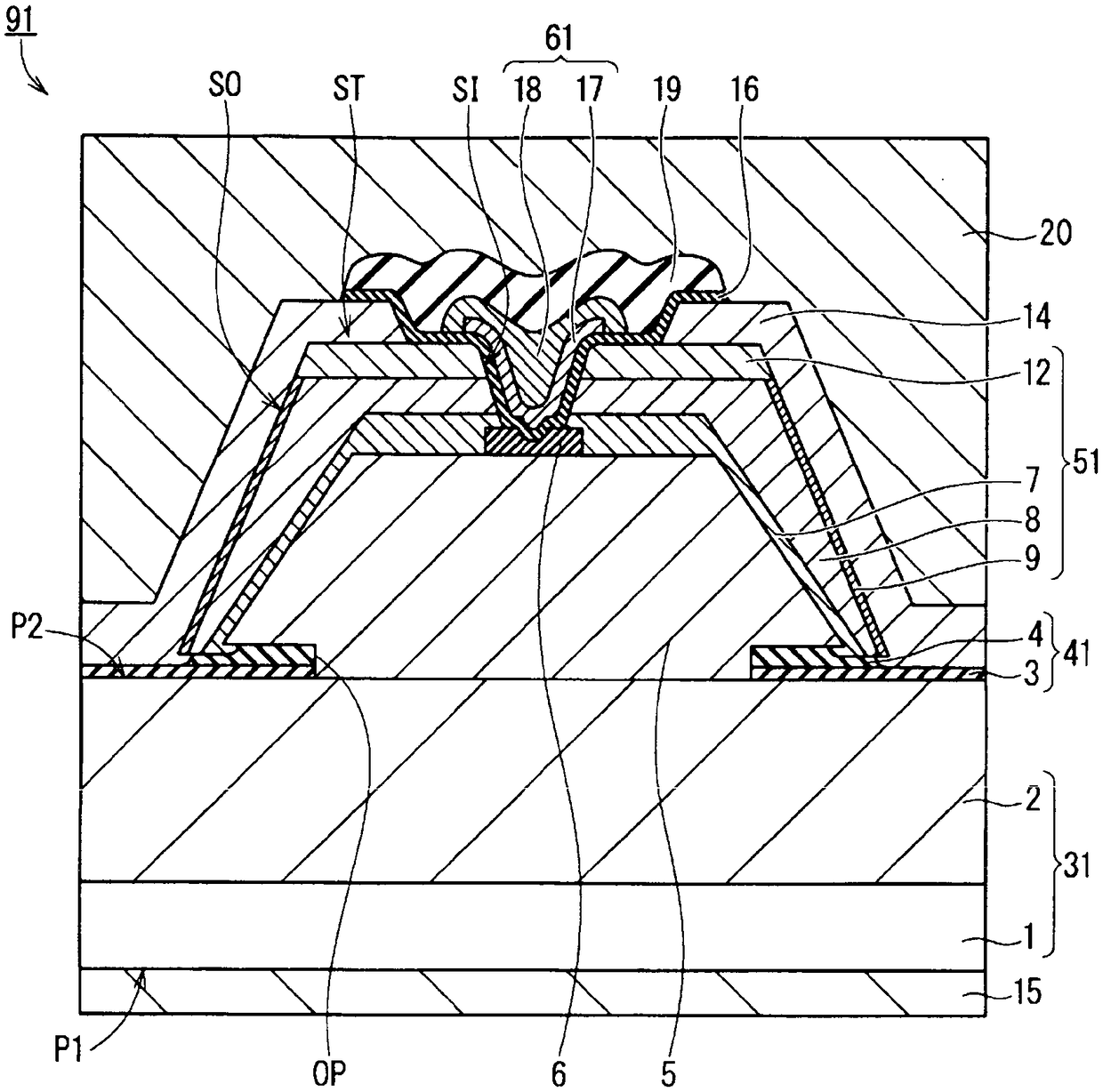
[0071] figure 1 It is a cross-sectional view schematically showing the structure of a semiconductor device (MOSFET) 91 according to this embodiment. The outline of the structure of the semiconductor device 91 will be described in (1) to (5) below.
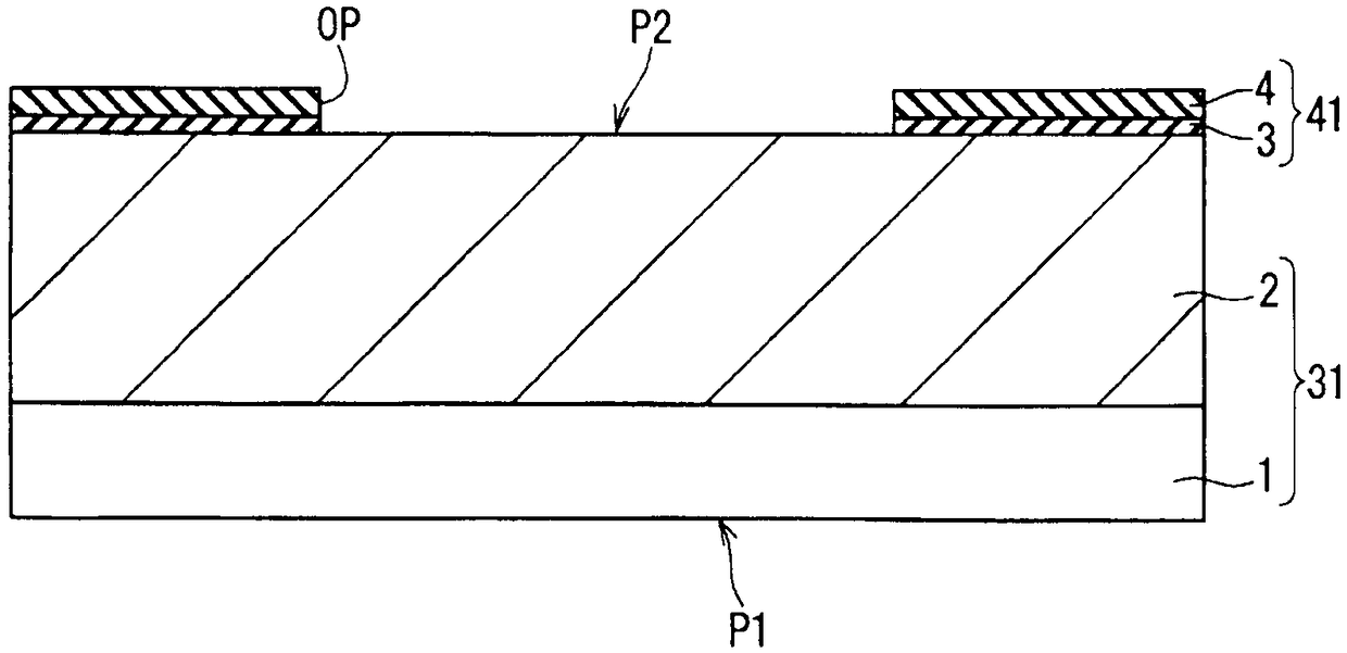
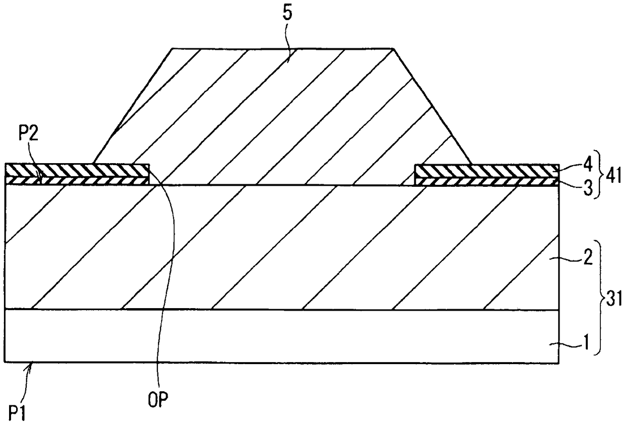
[0072] (1) The semiconductor device 91 has a semiconductor substrate (epitaxial substrate) 31, a first insulating layer 41, a second insulating layer 6, a laminated body 51, an n-type contact layer 12, a source electrode portion 14, a drain electrode 15, and a gate insulating film. 16 and the gate electrode 61. The semiconductor substrate 31 has a first surface (lower surface) P1 and a second surface P2 (upper surface) opposite to the first surface P1. The first insulating layer 41 is provided on the second surface P2 of the semiconductor substrate 31 and has an opening OP partially exposing the second surface P2. The second insulating layer 6 is provided on the second surface P2 of the semicondu...
Embodiment approach 2
[0156] Figure 27 It is a cross-sectional view schematically showing the structure of a MOSFET (semiconductor device) 92 according to this embodiment. MOSFET91( figure 1 : Embodiment 1) tends to increase the total thickness of the epitaxially grown layers. This is advantageous for obtaining a high withstand voltage, but on the other hand, since the resistance of the drift layer is high, the on-resistance tends to become high. Therefore, when priority is given to reducing the on-resistance, it is conceivable to reduce the drift layer resistance by omitting the bottom n-type epitaxial layer 5 of the MOSFET 91 like the MOSFET 92 . Accordingly, on-resistance can be reduced.
[0157] In the manufacturing method of MOSFET 92, the formation process of bottom n-type epitaxial layer 5 is omitted ( image 3 ). The process can thus be simplified. In addition, accompanying this omission, instead of the step of forming the second insulating layer 6 ( Figure 4 as well as Figure 5 ...
Embodiment approach 3
[0161] (summary of structure)
[0162] Figure 28 It is a cross-sectional view schematically showing the structure of the semiconductor device (diode) 93 of this embodiment. The outline of the structure of the semiconductor device 93 will be described in (1) below.
[0163] (1) The semiconductor device 93 has the semiconductor substrate (epitaxial substrate) 31 , the insulating layer 42 , the laminate 53 , the n-type barrier layer 12D, the anode electrode 25 and the cathode electrode 24 . The semiconductor substrate 31 has a first surface (lower surface) P1 and a second surface (upper surface) P2 opposite to the first surface P1. The insulating layer 42 is provided on the second surface P2 of the semiconductor substrate 31 and has an opening OP partially exposing the second surface P2. The laminated body 53 has an n-type epitaxial layer 7D and a p-type epitaxial layer 9D in this order on the second surface P2 of the semiconductor substrate 31 . The n-type epitaxial layer 7...
PUM
 Abstract
Description
Claims
Application Information
 - R&D
- Intellectual Property
- Life Sciences
- Materials
- Tech Scout
- Unparalleled Data Quality
- Higher Quality Content
- 60% Fewer Hallucinations
Browse by: Latest US Patents, China's latest patents, Technical Efficacy Thesaurus, Application Domain, Technology Topic, Popular Technical Reports.
© 2025 PatSnap. All rights reserved.Legal|Privacy policy|Modern Slavery Act Transparency Statement|Sitemap|About US| Contact US: help@patsnap.com


