Display device and driving method thereof
A driving method and technology of a display device, which are applied to static indicators, light guides, optics, etc., can solve the problem of insufficient color gamut to meet requirements, and achieve the effect of increasing the color gamut range.
- Summary
- Abstract
- Description
- Claims
- Application Information
AI Technical Summary
Problems solved by technology
Method used
Image
Examples
Embodiment 1
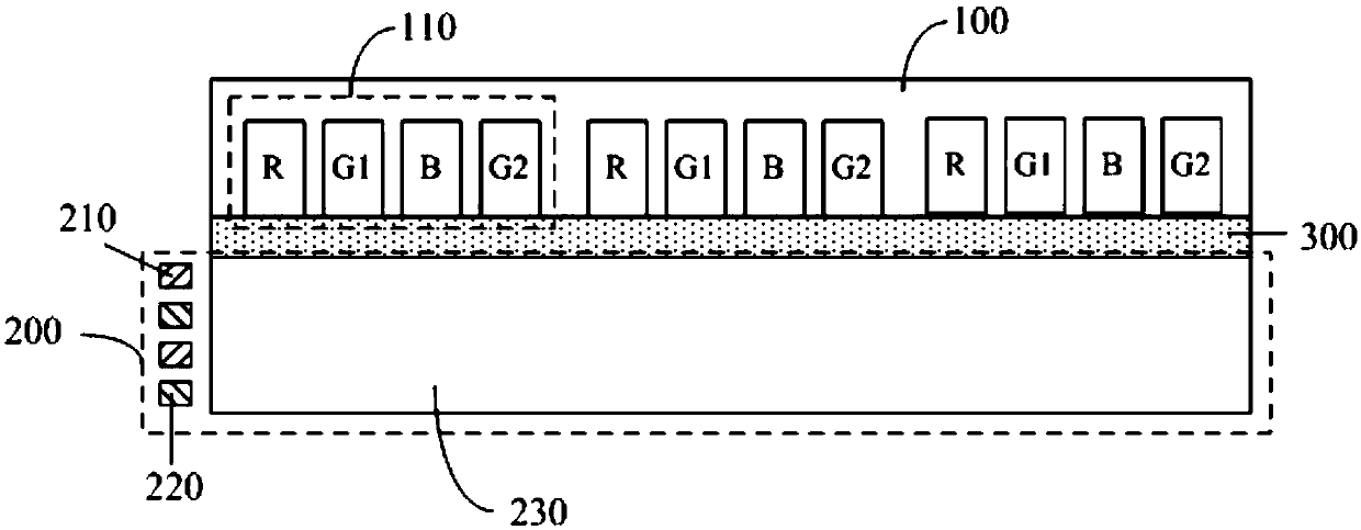
[0026] In specific implementation, the light source assembly may be a side-entry type. Such as figure 1 As shown, the light source assembly 200 may further include: a light guide plate 230 for guiding the light emitted by the green LED 210 and the blue LED 220 in the light source assembly to the liquid crystal display panel 100 . Moreover, the quantum dot layer 300 is located on the side of the light guide plate 230 facing the liquid crystal display panel 100 . The quantum dot layer 300 may include: a film substrate, green quantum dots and red quantum dots, and the green quantum dots and red quantum dots are evenly distributed on the surface of the film substrate. Of course, the light source assembly can also be a direct type, which is not limited here.
[0027] In specific implementation, the peak wavelength λ of the emitted light of the green LED GLED Can be 540nm. And the green LED can excite the red quantum dots and green quantum dots in the quantum dot layer, so that ...
Embodiment 2
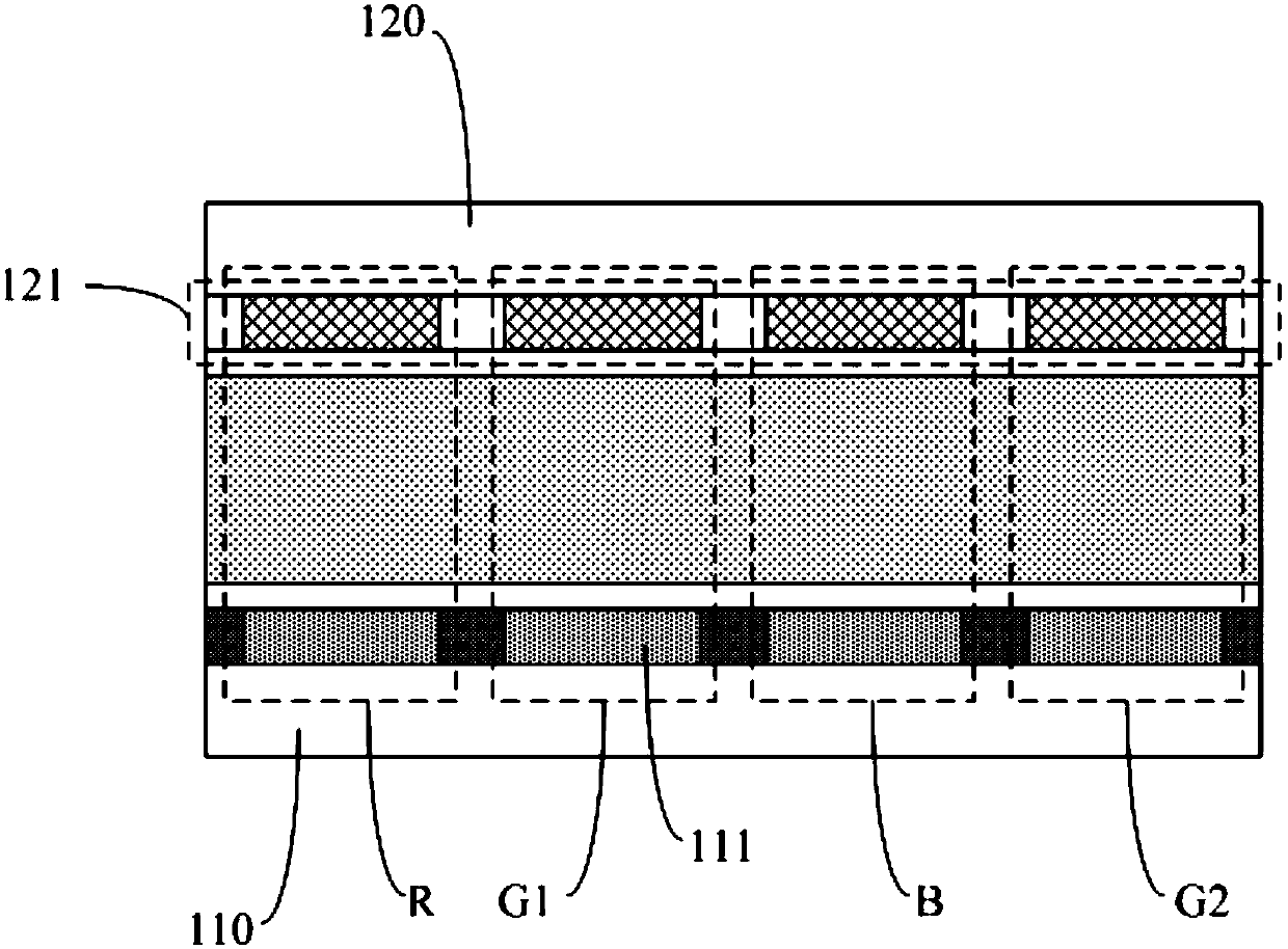
[0039] The structural schematic diagram of the display device corresponding to this embodiment is as follows Figure 5 As shown, it is modified for the implementation of the quantum dot layer and the liquid crystal display panel in the first embodiment. The following only describes the differences between this embodiment and the first embodiment, and the similarities will not be repeated here.
[0040] In specific implementation, such as Figure 5 As shown, the liquid crystal display panel may include: an array substrate 110 and an opposite substrate 120 disposed opposite to each other. The quantum dot layer 300 can be located between the array substrate 110 and the opposite substrate 120; wherein, the quantum dot layer 300 can be located on the opposite substrate 120, and is located on the side of the opposite substrate 120 facing the liquid crystal layer; or, the quantum dot layer 300 It can also be located on the array substrate 110 and on the side of the array substrate ...
PUM
 Abstract
Description
Claims
Application Information
 - R&D
- Intellectual Property
- Life Sciences
- Materials
- Tech Scout
- Unparalleled Data Quality
- Higher Quality Content
- 60% Fewer Hallucinations
Browse by: Latest US Patents, China's latest patents, Technical Efficacy Thesaurus, Application Domain, Technology Topic, Popular Technical Reports.
© 2025 PatSnap. All rights reserved.Legal|Privacy policy|Modern Slavery Act Transparency Statement|Sitemap|About US| Contact US: help@patsnap.com


