Passband Embedded Frequency Selective Absorber Based on Parallel LC Resonator Loading
A technology of frequency selection and wave absorber, applied in antennas, electrical components, etc., can solve the problems of complex structure of passband embedded frequency selection wave absorber, and achieve the effect of simple manufacturing process, simplified structure and reduced size
- Summary
- Abstract
- Description
- Claims
- Application Information
AI Technical Summary
Problems solved by technology
Method used
Image
Examples
Embodiment 1
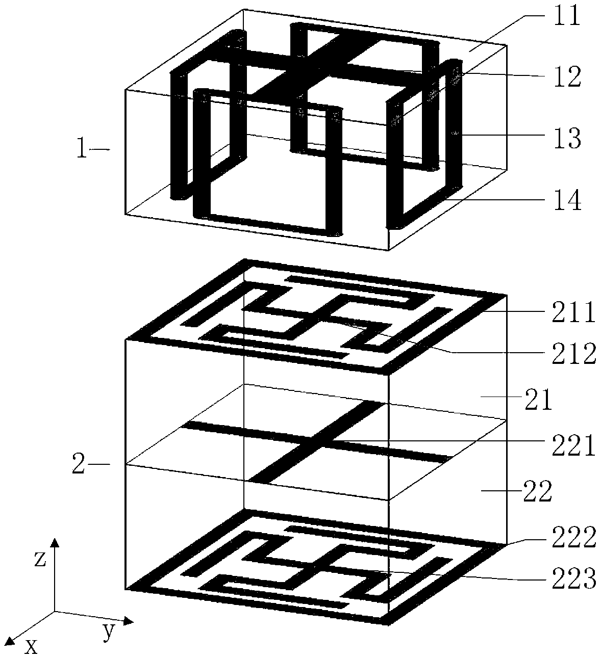
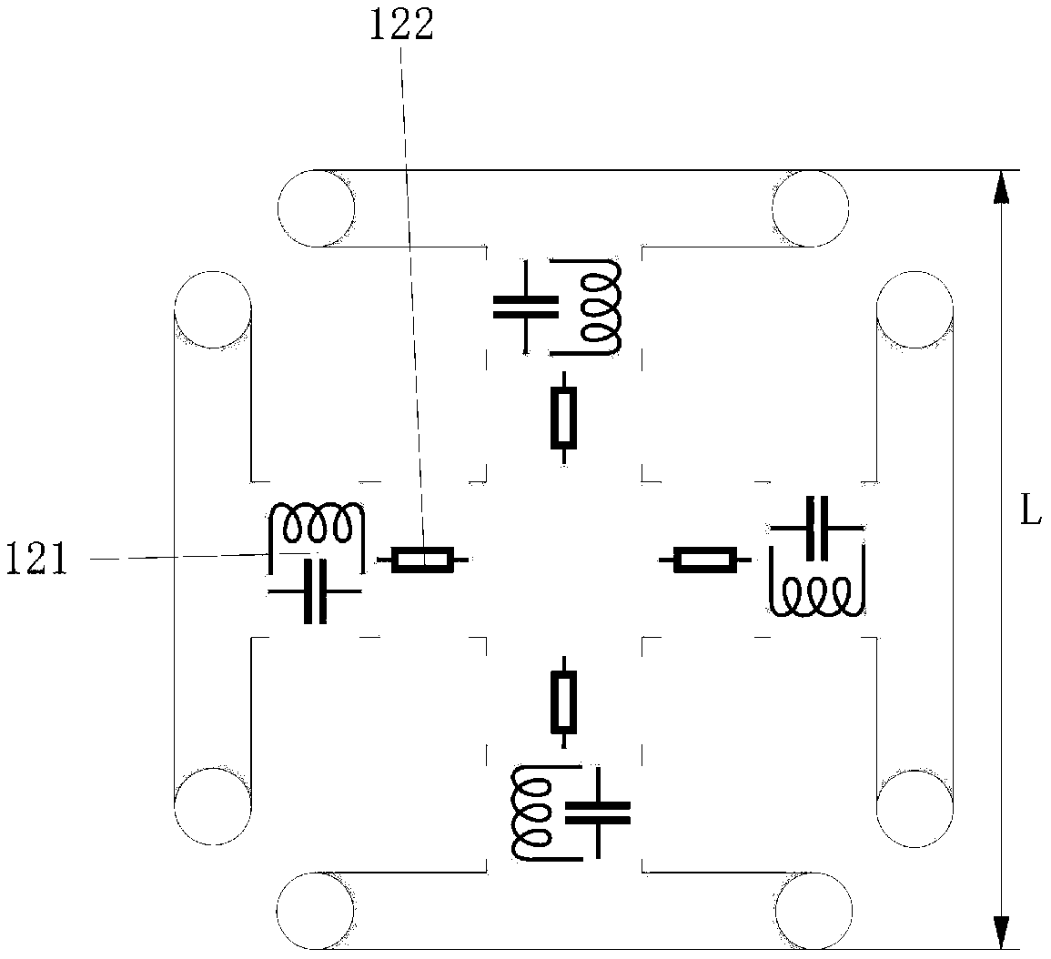
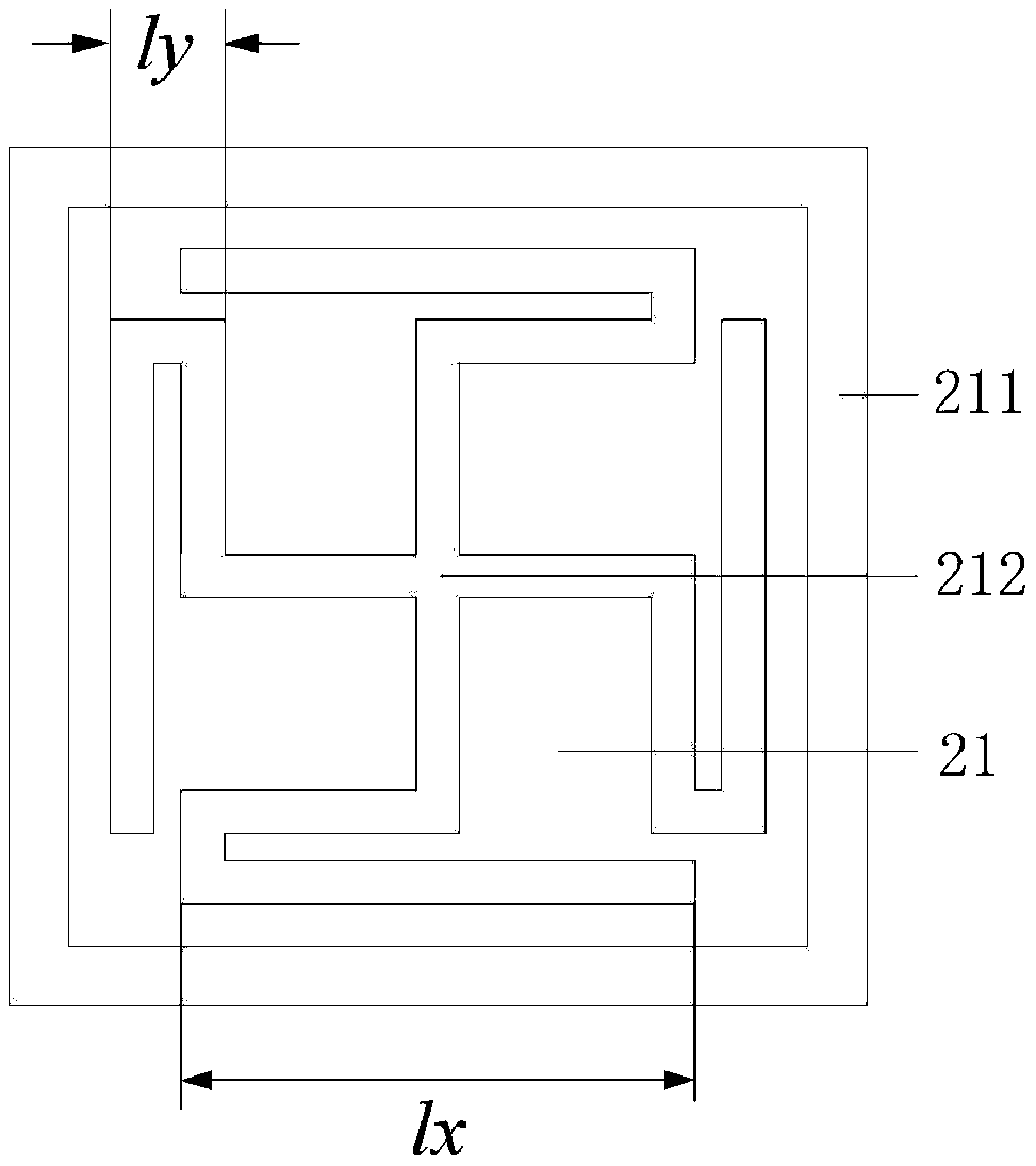
[0024] refer to figure 1 , a pass-band embedded frequency selective absorber loaded based on a parallel LC resonator, comprising m×n absorber units periodically arranged, m=30, n=30; the absorber unit includes The upper and lower passband embedded absorbing structure 1 and the bandpass frequency selection structure 2 are supported by nylon columns in the middle, and the air layer is set to 4.5mm. The passband embedded wave-absorbing structure 1 includes printed on the upper surface such as figure 2 The shown Jerusalem cross-shaped patch 12 and the first dielectric plate 11 with four strip-shaped patches 14 printed on the lower surface use a plate with a relative dielectric constant of 2.65 and a size of 6.6mm×6.6mm×1mm . The Jerusalem cross patch 12 as figure 2 As mentioned above, the center of the cross is located on the central axis of the medium plate, the total length L of the cross body is 6.6mm, the arm width is 1mm, and the length of the horizontal strip structure ...
Embodiment 2
[0029] The structure is the same as that of Example 1, only the following parameters have been adjusted:
[0030] Absorber m×n periodically arranged absorber units, m=6, n=6, the first dielectric plate 11, the second dielectric plate 21 and the third dielectric plate 22, with a side length of 9 mm and a thickness of 0.5mm, a square plate with a relative permittivity of 1.5, the resistance of the resistor 122 is 90Ω, the passband embedded absorbing structure 1, and the thickness of the air layer between it and the bandpass frequency selective structure 2 is 10mm.
Embodiment 3
[0031] The structure of embodiment 3 is the same as that of embodiment 1, only the following parameters have been adjusted:
[0032] Absorber m×n periodically arranged absorber units, m=100, n=100, the first dielectric plate 11, the second dielectric plate 21 and the third dielectric plate 22, the side length is 6.5mm, the thickness 1.5mm, a square plate with a relative dielectric constant of 5, the resistance of the resistor 122 is 210Ω, the passband embedded absorbing structure 1, and the thickness of the air layer between it and the bandpass frequency selective structure 2 is 2mm.
[0033] Below in conjunction with simulation experiment, technical effect of the present invention is described further:
[0034] 1. Simulation conditions and content:
[0035] 1) Place the absorber described in Embodiment 1 on the xoy plane, and use the commercial simulation software HFSS_15.0 to perform the above-mentioned embodiment 1 on the plane xoy plane where the transverse electric mode ...
PUM
| Property | Measurement | Unit |
|---|---|---|
| size | aaaaa | aaaaa |
| size | aaaaa | aaaaa |
| electrical resistance | aaaaa | aaaaa |
Abstract
Description
Claims
Application Information
 - R&D
- Intellectual Property
- Life Sciences
- Materials
- Tech Scout
- Unparalleled Data Quality
- Higher Quality Content
- 60% Fewer Hallucinations
Browse by: Latest US Patents, China's latest patents, Technical Efficacy Thesaurus, Application Domain, Technology Topic, Popular Technical Reports.
© 2025 PatSnap. All rights reserved.Legal|Privacy policy|Modern Slavery Act Transparency Statement|Sitemap|About US| Contact US: help@patsnap.com


