Rapid correction method of scanning electron microscope image drift
A scanning electron microscope, image drift technology, applied in image enhancement, image analysis, image data processing and other directions, can solve the characterization that affects the SEM size measurement performance, the difficulty of establishing a general model, and the difficulty of meeting real-time performance, etc., to achieve fast image drift. Correction, simple algorithm, real-time feedback effect
Inactive Publication Date: 2018-09-11
SUZHOU UNIV
View PDF4 Cites 5 Cited by
- Summary
- Abstract
- Description
- Claims
- Application Information
AI Technical Summary
Problems solved by technology
However, at high magnification, image drift caused by electron beam drift and electromagnetic interference will affect the size measurement and performance characterization of nanomaterials by SEM.
[0003] At present, scholars at home and abroad are actively investing in the correction method of SEM image drift, but the algorithm is complex and computationally intensive, it is difficult to meet the real-time requirements, and it is limited by the difficulty of establishing a general model for image drift correction.
Method used
View moreImage
Smart ImageViewing Examples

Examples
Embodiment
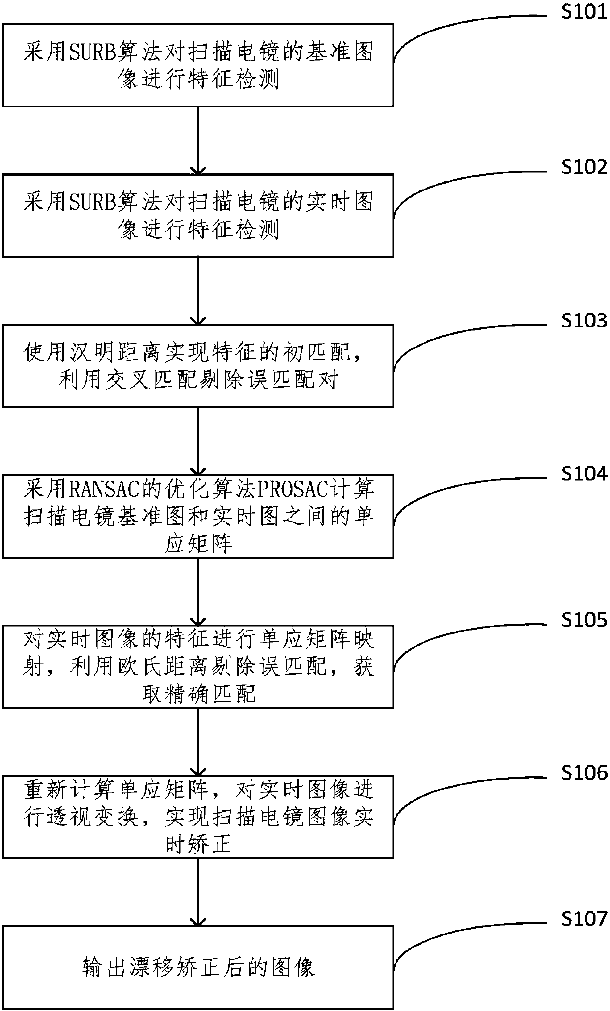
[0038] refer to figure 1 As shown, the present invention discloses a method for quickly correcting the image drift of a scanning electron microscope, comprising the following steps:
Login to View More PUM
 Abstract
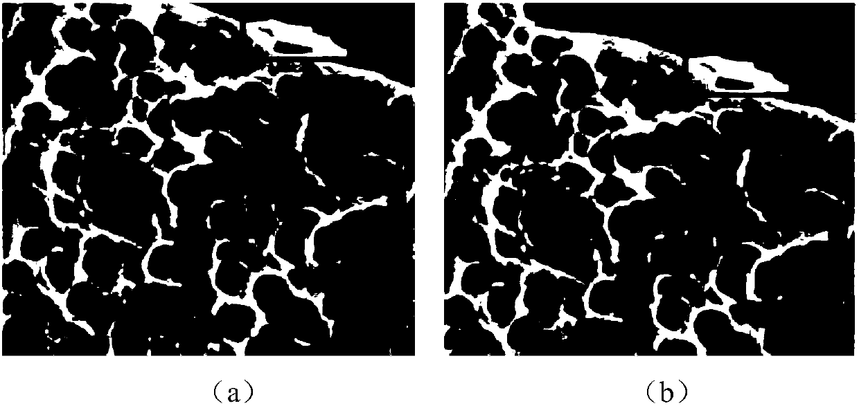
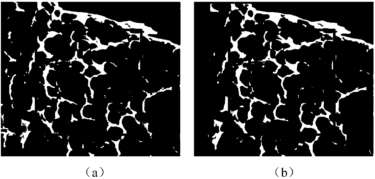
The present invention discloses a rapid correction method of scanning electron microscope image drift. The method comprises the steps of: performing feature detection of a reference image of a scanning electron microscope; performing feature detection of real-time images of the scanning electron microscope; performing feature first matching of a feature detection result of the reference image anda feature detection result of the real-time image, and rejecting a mistake matching pair; calculating and obtaining a homography matrix between the reference image and the real-time image; performinghomography matrix frame mapping of feature points of the real-time image, rejecting the mistake matching pair again, and obtaining an accurate matching pair; and recalculating and obtaining a homography matrix between the reference image and the real-time image, and performing perspective transformation of the real-time image. The rapid correction method is simple in algorithm and fast in speed, can achieve real-time feedback and is good in image drift correction effect.
Description
technical field [0001] The invention relates to the technical field of electron microscope image processing, in particular to a fast correction method for scanning electron microscope image drift. Background technique [0002] With the development of nanoscience, new nanomaterials and their excellent properties are constantly being discovered and recognized, and have shown very broad application prospects. Compared with the traditional optical microscope, the scanning electron microscope (SEM) has been widely used in the performance characterization of nanomaterials due to its simple sample preparation, wide adjustable magnification range, high image resolution, and large depth of field. measurement etc. However, at high magnification, image drift caused by electron beam drift and electromagnetic interference will affect the size measurement and performance characterization of nanomaterials by SEM. [0003] At present, scholars at home and abroad are actively investing in ...
Claims
Login to View More Application Information
Patent Timeline
 Patent Type & Authority Applications(China)
IPC IPC(8): G06T5/00G06T7/00
CPCG06T7/0002G06T2207/10061G06T5/80
Inventor 汝长海徐伟谷森朱军辉
Owner SUZHOU UNIV
Features
- R&D
- Intellectual Property
- Life Sciences
- Materials
- Tech Scout
- Unparalleled Data Quality
- Higher Quality Content
- 60% Fewer Hallucinations
Learn More Browse by: Latest US Patents, China's latest patents, Technical Efficacy Thesaurus, Application Domain, Technology Topic, Popular Technical Reports.
© 2025 PatSnap. All rights reserved.Legal|Privacy policy|Modern Slavery Act Transparency Statement|Sitemap|About US| Contact US: help@patsnap.com