


Quick Research
Generate reliable direction feasibility study reports for your R&D in just a few steps.

Technical Q&A
Discover and master advanced knowledge NOW. Basics, ideas, possibilities, all at once.

Find Solutions
As an expert in R&D theories, this can generate solutions to your technical problems instantly.

Evaluate Feasibility
Analyze your overall solution with one click, know your potential R&D risks in advance.

Monitor Landscape
Get weekly tech updates, stay abreast of the latest tech innovations and key insights.
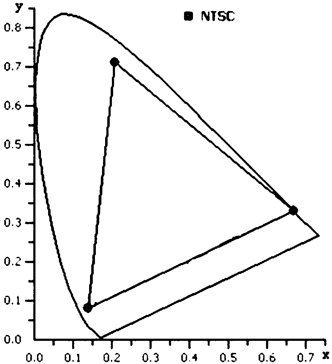
Organic electroluminescence device
An electroluminescent device and electroluminescent technology, which are applied to circuits, electrical components, electrical solid devices, etc., can solve the problem of insufficient color gamut of OLED devices, and achieve the effects of increasing the color gamut area, increasing the thickness, and enhancing the strength of the microcavity.
- Summary
- Abstract
- Description
- Claims
- Application Information
AI Technical Summary
Problems solved by technology
Method used
Image

Examples
Embodiment 1
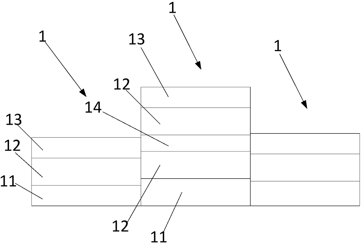
[0083] The embodiment of the present invention provides a specific example of an organic electroluminescence device. The organic electroluminescence device in this embodiment includes three types of monochromatic light-emitting organic light-emitting diodes with luminous wavelengths, namely red organic light-emitting diodes, green light organic light-emitting diodes and blue light organic light-emitting diodes. Among them, the three organic light emitting diodes all have a microcavity structure.
[0084] Each organic light emitting diode includes a first electrode layer, a light emitting layer and a second electrode layer which are stacked. Wherein, there are two light-emitting layers in the green organic light-emitting diode, and the two light-emitting layers are connected through a transparent connection layer, and the transparent connection layer is Li 2 CO 3 / HAT-CN / TAPC, the thickness is 40nm, and the refractive index is 1.8. Blue light and red light organic light emit...
Embodiment 2
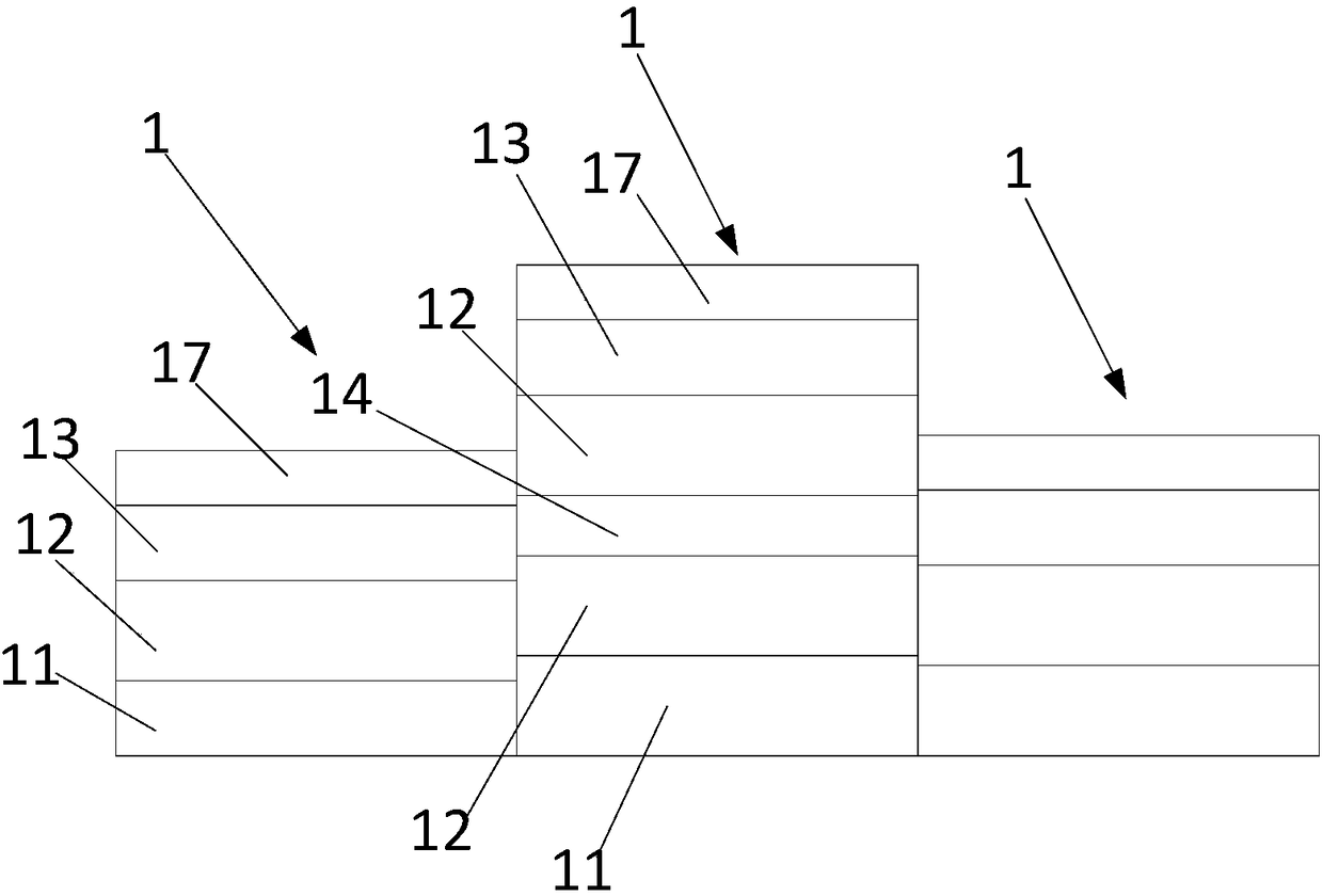
[0094] The embodiment of the present invention provides a specific example of an organic electroluminescence device. Its structure is the same as embodiment 1, and the difference with the organic electroluminescent device that embodiment 1 provides is:
[0095] The second electrode layer of the green organic light emitting diode includes two metal oxide layers stacked one on top of the other, and a metal layer arranged between the two metal oxide layers.
[0096] The device structure of the green organic light-emitting diode is: Ag(10nm) / ITO(160nm) / CuPc(20nm) / TPD(100nm) / CBP:Ir(ppy) 3 (10%,30nm) / TPBi(40nm) / Li 2 CO 3 (1nm) / HAT-CN(10nm) / CuPc(20nm) / TPD(100nm) / CBP:Ir(ppy) 3 (3%,30nm) / TPBi(40nm) / LiF(1nm) / MoO 3 / Ag / MoO 3(5nm / 5nm / 5nm) / NPB(60nm).
Embodiment 3
[0098] The embodiment of the present invention provides a specific example of an organic electroluminescence device. Its structure is the same as embodiment 1, and the difference with the organic electroluminescent device that embodiment 1 provides is:
[0099] The transparent connection layer is TAPC with a thickness of 1 nm and a refractive index of 1.8.
[0100] The device structure of the green organic light emitting diode in this embodiment is: Ag(10nm) / ITO(160nm) / CuPc(20nm) / TPD(120nm) / CBP:Ir(ppy) 3 (10%,30nm) / TPBi(40nm) / TAPC(1nm) / TPD(120nm) / CBP:Ir(ppy) 3 (3%, 30nm) / TPBi(40nm) / LiF(1nm) / Mg:Ag(20%, 15nm) / NPB(60nm).
PUM
 Abstract
Description
Claims
Application Information
 - R&D Engineer
- R&D Manager
- IP Professional
- Industry Leading Data Capabilities
- Powerful AI technology
- Patent DNA Extraction
Browse by: Latest US Patents, China's latest patents, Technical Efficacy Thesaurus, Application Domain, Technology Topic, Popular Technical Reports.
© 2024 PatSnap. All rights reserved.Legal|Privacy policy|Modern Slavery Act Transparency Statement|Sitemap|About US| Contact US: help@patsnap.com